Power module thermal design analysis
Summary: The surface of the power module is hot, the module is broken? ! Slow, a little bit hot, just because it is working hard. However, the high temperature has a great impact on the reliability of the power module! We must focus on thermal design to reduce the temperature rise of the power supply surface and internal components. This time, we took a look at the thermal design of the power module.
High temperatures have a significant impact on the reliability of power modules with high power density. High temperature will lead to a decrease in the life of electrolytic capacitors, a decrease in the insulation properties of transformer enameled wires, damage to transistors, thermal aging of materials, and loss of solder joints. Statistics show that for every 2 °C increase in electronic component temperature, reliability is reduced by 10%.
For the thermal design of the power module, it consists of two levels: reducing losses and improving thermal conditions.
First, the loss of components
Loss is the direct cause of heat generation, and reducing losses is fundamental to reducing heat. Some manufacturers in the market put the heating elements inside the module, so that the heat can not be dispersed, this method is a little self-deception. Reducing the loss and temperature rise of internal heating elements is the last word.
The key components of the thermal design of the power module are generally: MOS tubes, diodes, transformers, power inductors, current limiting resistors, etc. Its losses are as follows:
1. Loss of MOS tube: conduction loss, switching loss (opening loss and turn-off loss);
2. Loss of rectifier diode: forward conduction loss;
3, transformer, power inductor: iron loss and copper loss;
4. Passive components (resistors, capacitors, etc.): Ohmic heat loss.
Second, thermal design
In the early stages of design, thermal design should be considered in terms of solution selection, component selection, and PCB design.
1, the choice of program
The program will directly affect the overall loss and the overall temperature rise.
2, the choice of components
The selection of components not only needs to consider electrical stress, but also thermal stress, and leave a certain amount of derating. The derating level can refer to the "National Military Standards - Component Derating Guidelines GJB/Z35-93", which specifies the various levels of derating for various components. Designing a stable and reliable power supply is really incapable, and must be designed, derated, and verified according to the traits of each component. Figure 1 shows some component derating curves, which are reduced as the surface temperature increases.

Figure 1 Derating curve
The package of components has a great influence on the temperature rise of the device. MOSFETs in DFN packages are more susceptible to heat dissipation than MOSFETs in DPAK (TO252) packages due to process variations. In the former, under the same loss conditions, the temperature rise will be relatively small. Generally, the larger the resistance of the package, the higher the rated power, and the surface temperature rise will be smaller under the same loss conditions.
In the design, the resistor to be evaluated generally has a current limiting detecting resistor of the MOS transistor, a driving resistor of the MOS transistor, and the like. Current limiting resistors are typically used in packages of 1206 or larger and used in parallel. The loss of the drive resistor also needs to be considered, otherwise it may cause the temperature rise to be too high.
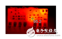
Sometimes circuit parameters and performance seem normal, but they actually hide a lot of problems. As shown in Figure 2, there is no problem with the basic performance of a certain circuit, but at room temperature, the infrared thermal imager is a test, and the surface temperature of the driving resistance of the MOS tube actually reaches 95.2 °C. In long-term work or high temperature environment, it is easy to have the problem of resistance burnout and module damage. It can be seen that it is especially important to use the thermal imager to test the temperature of the components during the development process, so that problems can be discovered and located in time. By adjusting the circuit parameters, the ohmic heat loss of the resistor is reduced, and the resistance package is changed from 0603 to 0805, which greatly reduces the surface temperature.

Figure 2 drive resistance surface temperature
3, PCB design
The copper area of ​​the PCB, the thickness of the copper skin, the material of the board, and the number of PCB layers all affect the heat dissipation of the module. The commonly used sheet FR4 (epoxy resin) is a good thermal conductive material, and the heat of the components on the PCB can be dissipated through the PCB. In special applications, there are also plates with smaller thermal resistance such as aluminum substrates or ceramic substrates.
The layout of the PCB also takes into account the heat dissipation of the module:
(1) The components with large heat should avoid the layout of the pile, do not “hotâ€, go where to make up, try to keep the heat evenly distributed on the board surface;
(2) Heat sensitive components should especially “what side is cool and which side to goâ€;
(3) Use a multi-layer PCB if necessary;
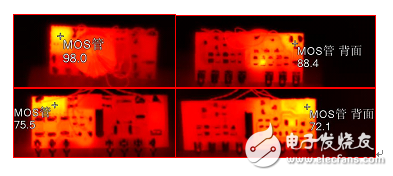
(4) The copper surface of the power component is cooled by heat, and the “hot hole†is used to transfer heat from one side of the PCB to the other. The pore size of the hot hole should be small, about 0.3mm, and the distance between the hot holes is generally 1mm~1.2mm. The method of applying a copper planar heating hole on the back of the power component can achieve a good heat dissipation effect and reduce the surface temperature rise of the power component. As shown in Figure 3, the above two figures show the surface temperature of the MOS tube and the temperature of the back PCB when this method is not used. The following two figures show the surface temperature of the MOS tube and the copper surface on the back side after the "back surface copper-coated planar heating hole" method. temperature. As can be seen:
a) MOS tube surface temperature is reduced by 22.5 ° C from 98.0 ° C;
b) The temperature difference between the MOS tube and the copper plane on the back side is greatly reduced, and the heat transfer performance of the heat hole is good.

Figure 3 Heat dissipation effect of the copper-clad heating hole on the back
When designing heat, you must also pay attention to:
1. For power modules with wide input voltage, the heat point and heat distribution of the high voltage input and low voltage input are completely different and need to be fully evaluated. The heat point and heat distribution during short circuit protection are also evaluated.
2. In the potting type power module, the potting compound is a good heat conducting material. The surface temperature rise of the internal components of the module is further reduced. Even so, we still have to test the surface temperature rise of internal components in high temperature environments to ensure module reliability. So how can we test the temperature rise of the internal components accurately? Please see "How ZLG tests the temperature rise inside the power module! In the article, there is a detailed description in the text.
The lcd projector is the product of the combination of liquid crystal display technology and projection technology. It uses the electro-optic effect of liquid crystal to control the transmittance and reflectivity of the liquid crystal unit through the circuit, thereby producing different gray levels and as many as 1670 million colors. Beautiful image. The main imaging device of LCD projector is liquid crystal panel. Led projector, generally refers to the light source of the projector is LED light source, the brightness is not high, within 500 lumens. The difference between dlp and led, most of them are in Projection field to distinguish.
lcd home projector,led lcd home projector,best home lcd projector,lcd home theatre projectors,best lcd home theater projector
Shenzhen Happybate Trading Co.,LTD , https://www.szhappybateprojectors.com