Design of 12-bit PWM DAC based on single chip microcomputer
[I. Introduction
In the transmitter type and controller type instrument made by single chip microcomputer, when it is required to output 1 - 5V or 4 - 20mA DC signal, a dedicated D/A chip is usually used, which is generally one piece per way. When the accuracy of the output signal is high, the number of bits of the D/A chip will also increase. In industrial meters, it is usually increased to 12 digits. The price of the 12-digit D/A is currently much higher than the price of the single-chip microcomputer, and the number of interface lines is also large. Especially in the case of isolation, the number of optocouplers required is equivalent to that of the interface line, resulting in a large increase in the number of components, resulting in an increase in volume and cost. If the D/A output is completed by PWM in the MCU-controlled instrument, the cost will be reduced to about one-tenth of the 12-bit D/A chip. We have adopted this approach in the S-Series flow meters and the results are very good. The following describes the principle of the PWM mode D/A.
[two]. Circuit principle
Generally, the accuracy of the 12-bit D/A converter in the manual is ±1/2LSB, and the comprehensive index of temperature drift is 20-50ppm/°C. The above two indicators can meet the requirements in the 0.2-level meter. The circuit given can achieve the above two indicators.
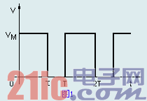
T in Fig. 1 is a fixed width, and the width of τ is variable. τ is divided into 5000 parts, 2us per serving. So the maximum value of τ τmax = 2 × 5000 = 10000us, which is the width of T. When τ=T, the duty ratio is 1, Vo=5.000V, and when τ=0, Vo=0V. The voltage obtained by this pulse voltage after two-stage RC filtering can be expressed by the following formula:

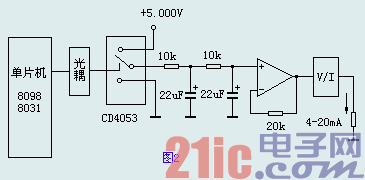
The VM must be a precision voltage source. Vo is proportional to the duty cycle and has a good linearity. This method is theoretically mature, but there are still some problems in practical applications. Figure 2 is the actual circuit, in which the MCU can use two common chips of 8098 or 8031, the value of VM is 5.000V±2mV, D/A and MCU must be electrically isolated. Otherwise, the interference generated by the digital pulse current will affect the D/A accuracy. From the oscilloscope, the interference glitch voltage of up to 50mV can be seen, so it is necessary to add optical isolation. The isolated pulse drives the analog switch CD4053. The CD4053 is a three-group two-contact analog switch. The common contact of the PWM pulse control switch is connected to +5.000V and ground. The PWM waveform is matched with the MCU output at the VI. The waveform is outputted by a voltage follower composed of an operational amplifier after two stages of RC filtering. The time constant of RC is generally taken as RC ≥ 2T, so that the two RCs add up to obtain a DC voltage with ripple less than 3mV. In this circuit, RC=220ms. If you want to further reduce the ripple, you can increase the product of RC appropriately. However, the response speed of the circuit will also slow down.

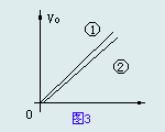
It is beneficial to use the op amp as a buffer for the RC filter output. It not only improves the load capacity of the filter circuit, but also improves the linearity. Through experiments, the buffering effect of this class of op amps is an important part of ensuring the accuracy and linearity of the entire D/A. Although the RC filter is unloaded and operates under very ideal conditions, Vo is not completely proportional to the duty cycle. After testing, there are some errors between Vo and the ideal value, as shown in Figure 3.

Curve 1 in the figure represents the ideal value, and curve 2 represents the measured value. As can be seen from the figure, the root of curve 2 is less than ideal. This is because the capacitor used is not a pure capacitor and contains a certain inductance. When the duty cycle is extremely small, since the pulse is very narrow, the frequency of the higher harmonics generated by the inductor is high, and the inductance is relatively strong against the higher harmonics, so at the position of the pulse edge, although the voltage varies greatly, However, the actual actual charging of the capacitor is small. This produces nonlinearity in the case of narrow pulses. When non-inductive capacitors are used, this nonlinearity is greatly improved, but it still cannot be completely matched. Since the capacity of the non-inductive capacitor is too small and the price is high, there is no practical significance in the large time constant filter circuit. The solution to this problem in practical use is to discard the nonlinear part of the root, using only the linear part. In industrial instruments, the standard signal is generally 1 - 5V or 4 - 20mA. The nonlinear part of curve 2 is below 0.4V, so when using 1 - 5V output signal, the accuracy of 0.03% fully meets the 12-bit D/A requirement.
KNLN6-63 Residual Current Circuit Breaker With Over Load Protection
KNLN6-63 TWO FUNCTION : MCB AND RCCB FUNCTIONS
leakage breaker is suitable for the leakage protection of the line of AC 50/60Hz, rated voltage single phase 240V, rated current up to 63A. When there is human electricity shock or if the leakage current of the line exceeds the prescribed value, it will automatically cut off the power within 0.1s to protect human safety and prevent the accident due to the current leakage.
leakage breaker can protect against overload and short-circuit. It can be used to protect the line from being overloaded and short-circuited as wellas infrequent changeover of the line in normal situation. It complies with standard of IEC/EN61009-1 and GB16917.1.
KNLN6-63 Residual Current Circuit Breaker,Residual Current Circuit Breaker with Over Load Protection 1p,Residual Current Circuit Breaker with Over Load Protection 2p
Wenzhou Korlen Electric Appliances Co., Ltd. , https://www.zjthermalrelay.com