Wanrun Technology: Transforming digital marketing, it’s imperative
LED packaging companies are resolutely transforming digital marketing. Founded in 2002, Wanrun Technology is a leading provider of medium and high-end LED light source device packaging and LED application lighting products integrating R&D, design, production and sales. The company provides customers with high quality LED light source devices and LED applications. An "integrated" solution for lighting products. Since 2013, the LED industry as a whole has seen an increase in revenues without increasing profits. For the company's future development and continued competitiveness, the company decided to transform digital marketing.
Divided into a huge cake of digital marketing, starting with the acquisition of the company. The company is firmly optimistic about digital marketing: full market space; high-speed growth; the business sector is relatively stable and clear. In August 2014, the company acquired a 100% stake in Rishang Optoelectronics. Rishang Optoelectronics is a leading company in the field of LED advertising signage lighting in the country. It is a downstream LED company, mainly engaged in outdoor advertising signage lighting systems such as airports and stations, and decided to transform digital marketing in this year. The acquisition of Sunshine Optoelectronics will help the company to quickly enter the LED advertising logo lighting professional market, achieve resource sharing, complement each other's advantages, enhance the core competitiveness of the company's lighting business, and achieve leap-forward development.
“Two-in-one participation†is ambition, aiming to build a digital marketing industry-wide ecological chain. Announced in November this year, the company plans to acquire a 100% stake in Dingsheng Yixuan and Yiwan Wireless. At the same time participate in the Botu advertising. The three Internet companies invested are mainly engaged in advertising business. Therefore, in order to accelerate the realization of the “upstream creative planning-data mining (DSP)--advertising-media†digital marketing industry chain development, the company's future key M&A direction is creative planning. , DSP, media three directions.
Company recommendation logic:
1) Transform digital marketing based on the original LED business. The LED business will become a source of stable income and profit, and an independent team will be launched in the future to launch a digital marketing business.
2) The team has strong execution and the new business is effectively carried out. The company has two M&A teams, two investment directors, and 8-10 main business mergers and acquisitions. Among them, Mr. Huang Gang, the investment director, is a professional in Internet communications.
3) The team structure is stable and the benefits are bundled. The company's non-public issuance of 700 million in April, of which 400 million by the controller, company executives, middle-level subscription, the company's development team is full of confidence. The recent shareholder reduction of non-corporate factors is a personal act.

10 Layer PCB Stack Up thickness, Design and manufacturing
Usually, 10 layer PCB is HDI PCB Board , but some are not.
10 Layer PCB Stack Up And Design
Regardless of the number of layers constituting the circuit board design, pad spacing, clearance, trace widths, copper weights and drill hole sizes must be tailored to your contract manufacturer (CM). If your design requires multiple layers, you need to consider additional DFM specifications for signals through vias, power and ground wiring, and PCB stackup.
For 10-layer PCB Manufacturing, it is necessary to determine the number of layers, their arrangement or stacking, and the type of material. These choices require coordination between thickness constraints; material parameters; such as dielectric constant, thermal expansion coefficient and electrical strength; signal type isolation and drilling options. For PCB Assembly , wiring options and their impact on welding process are very important. The function of CM limits the choice of vertical aspect of design.
When your PCB needs six layers of routing, you should choose to use ten layers of PCB. Because ten-layer circuit boards usually have six signal layers and four planes. Of course, we do not recommend the design of more than six signal layers on the 10-layer circuit board. Ten layers are also the largest number of layers, which can be easily manufactured on 0.062 inch thick sheets. Occasionally you will see a 12-layer PCB made of 0.062 inch thick board, but there are not many manufacturers who can make 12-layer circuit boards. Just right, besides making 10-layer circuit boards, we also have very rich experience in manufacturing 12-layer circuit boards.
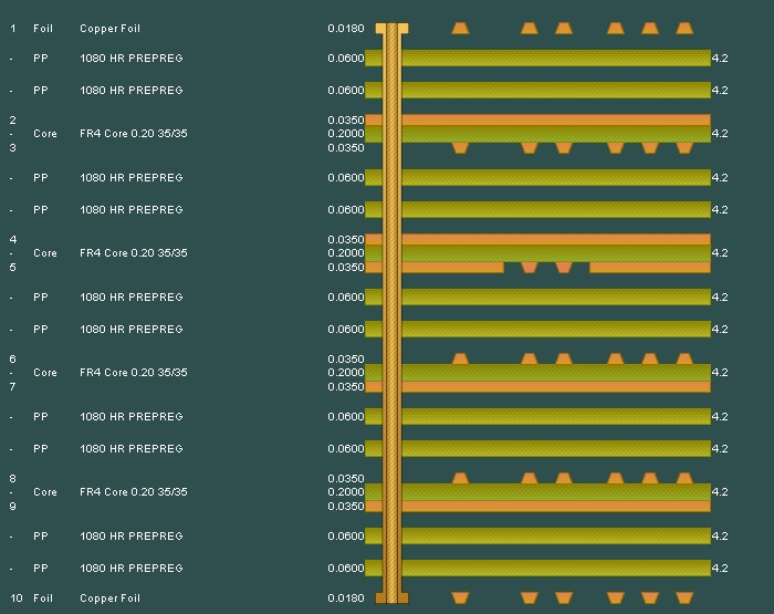
High layer count boards (10 +) require thin dielectrics (usually 0.006 or smaller on 0.062 thick plates), so they are automatically tightly coupled. After stacking and wiring properly, they can meet all our goals and have excellent EMC performance and signal integrity.
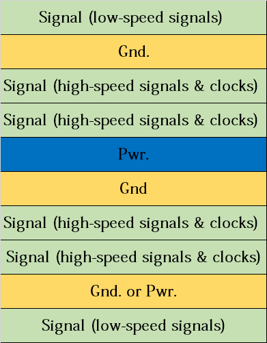
The reason why this stack has such good performance is the tight coupling between signal and return plane, the existence of high-speed shielding signal layer, multiple grounding layers, and tightly coupled power supply/grounding layer pairs in the center of circuit board.
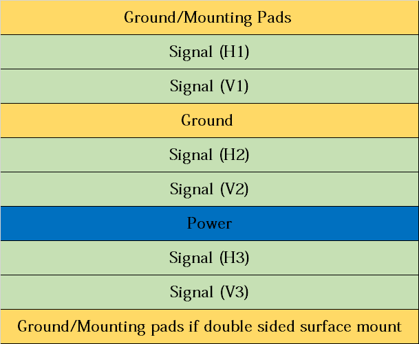
This 10-layer PCB stacking up method abandons closely spaced power/ground pairs. In return, it provides three signal routing layer pairs, shielded by the ground layer on the outer layer of the board, and isolated from each other through the internal power supply and the ground layer.
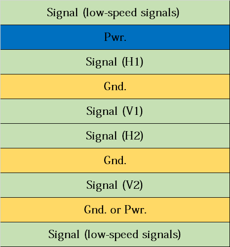
This 10-layer PCB stackup allows the routing of orthogonal signals near the same plane, but in the process, the closely spaced power/ground plane must also be abandoned.
In addition, we list some other stacking methods of 10-layer circuit boards for your reference.
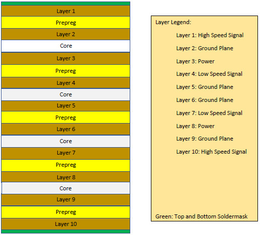
10 Layer PCB Thickness
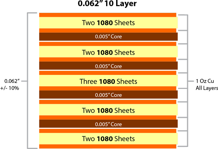
0.062''10 Layer PCB Stackup thickness
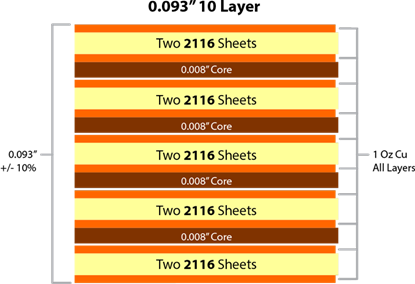
0.093'' 10 Layer PCB Stack UP thickness
10 Layer Stackup - 1.6mm thickness
layer order
layer name
material type
material description
dielectric constant
thickness
copper weight
1
top
copper
signal
0.035mm
1 oz
7630
prepreg
4.7
0.2mm
2
inner 1
copper
plane
1 oz
core
4.6
0.2mm
3
inner 2
copper
plane
1 oz
2116
prepreg
4.5
0.12mm
4
inner 3
copper
plane
1 oz
core
4.6
0.2mm
5
inner 4
copper
plane
1 oz
2116
prepreg
4.5
0.12mm
6
inner 5
copper
plane
1 oz
core
4.6
0.2mm
7
inner 6
copper
plane
1 oz
2116
prepreg
4.5
0.12mm
8
inner 7
copper
plane
1 oz
2116
prepreg
4.6
0.2mm
9
inner 8
copper
plane
1 oz
7630
prepreg
4.7
0.2mm
10
bottom
copper
signal
0.035mm
1 oz
Final board thickness: 1.6mm±0.16mm
10 Layer PCB Application
With the rapid development of today's increasingly complex multi-layer PCB, machines and equipment in various industries - commerce, industry, medicine, government, Aerospace - continue to grow in terms of speed, capacity, compactness and ease of use.
8, 10 and 12 layers of multi-layer PCB are useful in many high-tech equipment and computer systems. In recent decades, the development of multi-layer Printed Circuit Boards has led to the rapid development of computer technology - from the previous Gigabit system to today's GHz machine.
Especially 10-layer PCB, which is widely used in the following industries: Preamplifier, Satellite Dish, GPS Tracking Devices, SAN Storage, AC Drives, GSM Signal Booster, Mobile Broadband Router, Inverter 220V, Memory Module, Automotive dashboards
Cheap 10 Layer PCB manufacturing services
For customized printed circuit boards, our 10-layer PCB offers the fastest turning time for the best price we can offer. For on-demand pricing and ordering of your next Printed Circuit Board project, you can contact our online customer support or send us an email to get 10-layer PCB quotation immediately.
10 Layer PCB
Printed Wire Board,Custom PCB Board,10 Layer PCB,10 Layer PCB Stackup
JingHongYi PCB (HK) Co., Limited , https://www.pcbjhy.com
