High brightness LED driver controller application
The MAX16801A/B and MAXl6802A/B use a constant current to drive the HB LEDs in general lighting and display applications to provide the required control. The MAX16801A/B is suitable for general purpose AC input LED drivers , while the MAX16802A/B is specified for low voltage (10.8 to 24 V) DC input LED drivers . The HB LED driver circuit control IC consisting of MAX16801A/B and MAX16802A/B is mainly used in LCD TV and LCD monitor RGB backlighting, commercial and industrial lighting , decoration and construction.
1, the main features
The main features of the MAX16801A/8 and MAX16802A/8 are as follows:
Suitable for use as a Buck, Boost, Flyback, SEPIC and other circuit topologies; output power up to 50 W or more; internal error amplifier with 1% accuracy; PWM or linear dimming; 262 kHz (1±12%) fixed switching frequency operation; provides thermal shutdown and digital soft-start, programmable input startup voltage; startup supply current is typically 45μA, operating supply current is typically 1.4 mA; thin 8-pin μMAX Package.
2, pin function and internal structure
The pinouts of the MAX16801A/B and MAX16802A/B are shown in Figure 1. The notes list the functions for their individual pins. The MAX16801A/B and MAX16802A/B integrate a 1.23 V bandgap reference, digital soft-start, UVLO, voltage regulator, 262 kHz oscillator, error amplifier, CPWM comparator, current limit comparator, thermal shutdown, and MOS gate Unit circuit such as driver, as shown in Figure 2
Figure 1 Pin Arrangement
Note: Pin 1: External Programmable Undervoltage Lockout (UVLO), UVLO programming input enable voltage; this pin ground IC enable
Pin 2: Low Frequency PWM Dimming Input / Error Amplifying Inverter Input
Pin 3: Error amplifier output; this pin is connected to the DIM/FB compensation component in high-frequency precision LED current regulation.
Pin 4: current-regulated current sensing terminal, to eliminate the leading edge spike, the upper end of the sensing resistor is connected to an RC filter
Pin 5: Power Ground
Pin 6: Connect the external N-channel MOSFET gate
Pin 7: Gate drive power supply, connect a 10uF decoupling capacitor to GND
Pin 8: IC power supply application terminal, connect a decoupling capacitor of not less than 10uF to GND
Figure 2 Internal structure of the MAX16801A/B and MAX16802A/B
3, application circuit and working principle
3.1 Offline non-isolated flyback LED driver using MAX16801
Figure 3 Offline non-isolated flyback HB LED driver circuit with MAX16801
Offline isolated regression LED driver circuit with programmable input start-up voltage
3.1.1 Input Startup Circuit
The wake-up threshold of the MAX16801 pin UVLO/EN is 1.28 V. The voltage on this pin is only 1.28 V and the circuit can start working. Resistor dividers (R2 and R3) can be used as programming input startup voltages.
The MAX16801 has a built-in bootstrap UVLO circuit with large hysteresis that is useful for designing high-voltage HB LED drivers. When VIN exceeds the threshold level of 23.6 V, the circuit starts. During startup, the UVLO circuit keeps the CPWM comparator, ILIM comparator, oscillator, and output driver off to reduce current consumption. Once VIN reaches 23.6 V, the CPWM and ILIM comparators and oscillators are turned on and the output driver switches are allowed. If VIN drops below 9.7 V, the comparator, oscillator, and output driver are turned off.
High Precision Multilayer PCB|multilayer printed circuit board
Product name:
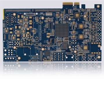
Industrial control board
Characteristic:
1, the board design
integration is very high;
2, the need to use composite
surface treatment method, gold finger plating hard gold 30 uinch;
3, gold finger position plate
thickness tolerance 1.6mm+/-0.10mm, it is recommended that customers in the
design of the gold finger corresponding to the inner line of the copper block,
in order to facilitate the plate thickness tolerance control.
Specifications:
Layer count: 6
Board thickness: 1.60mm
Base materials: FR4 S1141
Finished size: 172*148mm
Surface finish: Gold Plated +
finger
Line width/line space: 5/5mil
Minimum hole: 0.25mm
Solder resist color: blue
Cu thickness: inner layer 1 OZ
outer layer 1 OZ
Product name:
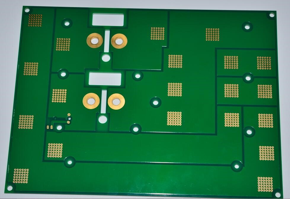
Thick Copper Board
Characteristic:
Prominent features: the outer
layer of copper thickness of 6 OZ, the inner product of copper thickness 6 OZ,
commonly used in large power equipment.
Processing difficulties:
1, inside and outside the need
to increase the thickness of copper thickness of 2 OZ or more by electroplating
method;
2, before pressing the need to
fill in the inner layer of resin;
3, the inner and outer layer
circuit is difficult to etch;
4, solder resist the need for
multiple printing.
 Specifications:
Layer count: 4
Board thickness: 3.0mm
Base materials: FR4 S1000-2
Finished size: 175*104mm
Surface finish:
Line width/line space:
12/12mil
Minimum hole: 0.5mm
Solder resist color: Sensitive
green
Cu thickness: inner layer 6 OZ outer layer 6 OZ
Product name:
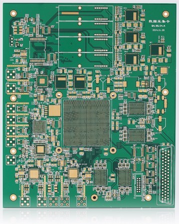
Data acquisition board
Characteristic:
1, the integration of the
board design is very high, thick diameter ratio of more than 10:1, heavy copper
plating is difficult;
2, the use of TG 170 plate
production.
Specifications:
1, the integration of the
board design is very high, thick diameter ratio of more than 10:1, heavy copper
plating is difficult;
2, the use of TG 170 plate
production.
Layer count: 8
Board thickness: 4.0mm
Base materials: FR4 S1000-2
Finished size: 400*400mm
Surface finish: mmersion
Line width/line space: 5/5mil
Minimum hole: 0.35mm
Solder resist color: Sensitive
green
Cu thickness: inner layer 1 OZ
outer layer 1 OZ
About Us:
BentePCB is a professional PCB manufacturing which is focus on double side, multilayer, HDI PCB , rigid PCB and Flexible PCB mass production. The company was established on 2011.
We have two factories together, The factory in Shenzhen is specialized in small and middle volume orders and the factory in Jiangxi is for big volumn.
Why Us?
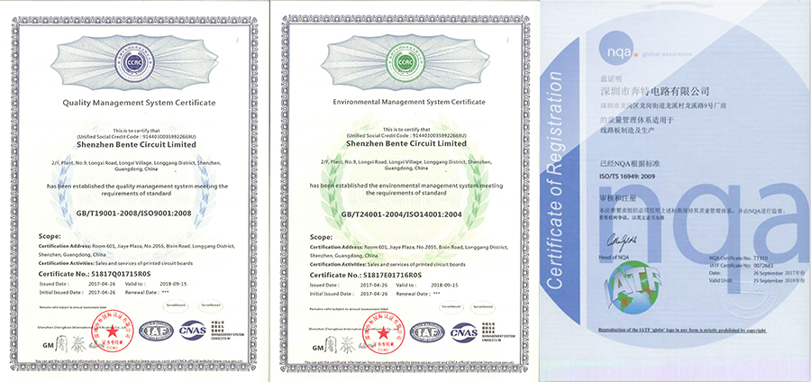
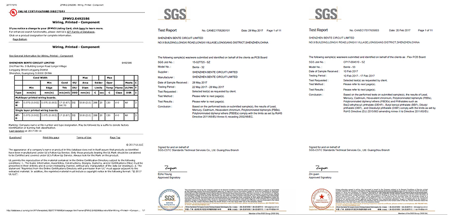
UL (E492586), ISO9001, ISO14001, TS16949, RoHS certified.
Turnover USD 10-50 million per year.
15,000 sqm area, 450 staff .
Mass Production from single to 16 layers.
Special Material:ROGERS, Arlon, Taconic.etc.
Client:Huawei, SAMSUNG, Malata, Midea,Texas Instruments.etc.
Certification(UL:E492586, TS16949, ISO14001, ISO9001,RoHS):
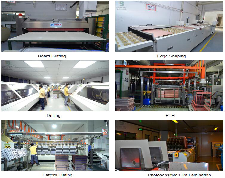
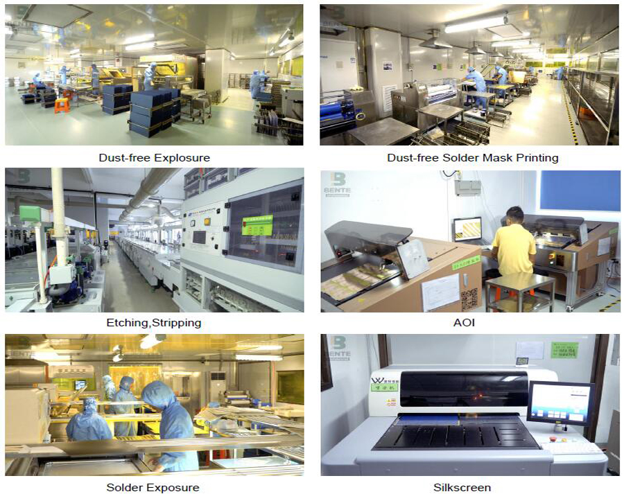
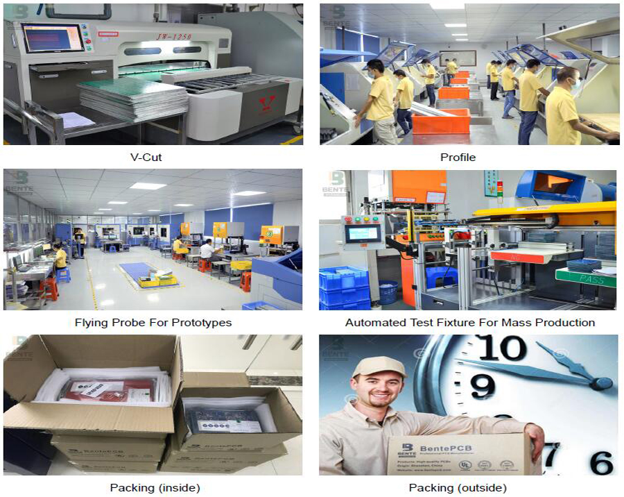
Factory Tour:
Exhibition:
We Took part in the famous exhibitions over the past years,and got highly appreciation from the top experts,as well as cooperated tightly with them.

Delivery:
BentePCB offers flexible shipping methods for our customers, you may choose from one of the methods below.


We don`t just sell PCBs .We sell sleep.

High Precision Multilayer PCB
High Precision Multilayer PCB, Multilayer Printed Circuit Board, Half Hole High-Precision Multilayer Board, High Precision Multilayer Board
Shenzhen Bente Circuit Limited , http://www.bentegroup.com