Protect sensitive and expensive loads with active output discharge
Power Products Division
Senior Product Marketing Engineer
Steve Knoth
Background InformationLinear regulators are commonly used in many modern electronic systems. Although low dropout (LDO) linear regulators are rarely the most expensive system components, they are often one of the most valuable components in terms of cost/benefit. One of the tasks of the LDO is to protect downstream loads from damage due to harsh environmental conditions such as temperature drift, voltage transients, power supply noise, voltage reversal, current surges, and EMI or ESD. In short, the design must be rugged and reliable, and include all the protection needed to mitigate environmental impact while protecting the load. Many low-cost LDO linear regulators do not contain the necessary protection features and therefore do not provide protection, often causing not only damage to the regulator, but also damage to the load.
Image sensor systems are a typical example of the need to protect expensive and sensitive loads. Image sensors typically contain sophisticated, expensive digital ICs that take images and convert them directly into digital images. The two most popular image sensors are charge coupled device (CCD) and CMOS imagers. Various devices, such as endoscopes and security cameras, include image sensors.
Some applications require control of the power cycle during power up and power down. In multi-rail systems, FPGAs, ASICs, DSPs, microprocessors, and other digital ICs require multiple voltage rails to be turned on and off in a specific order. Otherwise, these ICs may be damaged, or the system's power-on reset logic may be corrupted. If not sorted correctly, it can have disastrous consequences. For systems that must control the output state, high-reliability systems such as military, avionics, or aerospace are typical examples, especially if the supply voltage is required to cycle continuously and on.
The LDO can use the active output discharge function to meet the system's power-down requirements. The active output discharge function allows the LDO's output to be discharged quickly without having to rely on the LDO's load or the LDO's resistor divider to discharge the output. If the input voltage is removed, or if the shutdown function is enabled, the LDO with active output discharge can quickly pull down the output voltage with an NMOS switch. The main advantage of devices with active output discharge is that the output is in a known state when power is removed. Regardless of the load state, the output of such devices is always discharged as expected. For applications that require accurate power sequencing when shutting down (eg, image sensors and microcontrollers), it is important to be able to actively discharge the discharge.
Comparison of Low Dropout Linear Regulator (LDO) with Other RegulatorsLow-voltage step-down conversion and regulation can be achieved in a variety of ways. Switching regulators operate at high efficiency over a wide range of voltages, but require magnetic components and capacitors to operate, thus occupying a relatively large board space. A charge pump (or switched capacitor voltage converter) can be used to achieve a lower voltage conversion, but the output current capability is limited and requires an external capacitor to operate and stabilize. Low dropout linear regulators are generally less efficient, but produce less noise and are easier to use for buck applications. However, modern design methods and chip fabrication processes have enabled low dropout linear regulators (LDOs) to go deeper into buck applications. Low dropout linear regulators now feature ultra-fast transient response, low dropout voltage, low voltage operation (typically as low as 0.6V), high output current capability, and the ability to operate from a single supply.
The current generation of fast, high-current, low-voltage digital ICs (such as FPGAs, DSPs, CPUs, and ASICs) imposes stringent power requirements for powering the core and I/O channels. However, these digital ICs are not stable enough from a power supply perspective. Traditionally, high-efficiency switching regulators have been used to power these devices, but switching regulators can have potential noise interference problems as well as transient response and layout constraints. As a result, LDOs are finding the way to use them, and in such applications and other low-voltage conversion systems, they are finding their way. The trend is changing due to recent product innovations and enhancements, and the new LDOs rarely require a compromise in performance.
LDO design challengeA large number of industry-standard linear regulators operate with a single voltage source with low dropout voltage, but most regulators cannot provide very low voltage and output noise conversion (output as low as 0.6V), wide input/output voltage range, and wide Protection function. The PMOS LDO is capable of operating with a single low supply with low dropout voltage, but is limited by the pass transistor VGS characteristics and the input voltage cannot be very low. NMOS-based devices provide fast transient response, but require two power supplies to bias the device. The NPN regulator provides a wide range of input and output voltages, but requires two supply voltages or large differentials. In contrast, PNP regulators, if properly architected, can achieve very low dropout voltages, high input voltages, low noise and low voltage conversion with a single power supply, and provide reliable protection.
As process technology nodes continue to shrink, modern digital ICs need to operate at lower voltages. For many existing input voltage rails, operating at higher currents and lower output voltages means that the power consumption from the linear regulator increases. The increased power consumption is directly converted into heat. Therefore, the latest packaging methods are needed to minimize the temperature rise inside the regulator and limit the thermal issues of the application. In addition, linear regulators that operate with low dropout voltages (minimizing the difference between the input and output voltages while the regulator maintains regulation and stability of the output) reduce power consumption and therefore reduce thermal issues.
Two other challenges are the high power supply ripple rejection ratio (PSRR) and low output voltage noise. Devices with high power supply ripple rejection ratios easily filter out and reject noise from the input, resulting in a clean, stable output. In addition, devices with very low output voltage noise over a wide bandwidth are beneficial for today's voltage rails because noise sensitivity is a factor to consider for modern voltage rails. High current, low output voltage noise is clearly a necessary performance requirement.
Some industrial LDOs provide active output discharge to protect the load. However, existing solutions only start when the device is turned off. Until now, it has been difficult to find a circuit design that has a "dual" effect to actively discharge the discharge, that is, the function can be activated when the input voltage is pulled low.
A new single-supply linear regulatorObviously, an active output discharge LDO should have the following characteristics:
• Operate on a single power supply (for ease of use)
• Fast transient response time
• Operates over a wide range of input/output voltages
• Can provide a large output current
• Low output noise
• Operate at very low differential pressures
• Excellent thermal performance
• High PSRR over a wide frequency range
• Active output discharge circuit has a complete dual role - valid when SHDN or VIN is pulled low
Fortunately, Linear Technology recently introduced the 500mA LT3066 low dropout linear regulator with active output discharge, which has all of the necessary attributes described above. Some applications require that the output state is known at turn-off and the LT3066 is designed to meet this requirement. Its output is always discharged as expected, regardless of the state of the load.
The LT3066 is a high voltage, low noise, low dropout voltage linear regulator that provides accurate, programmable current limit, active discharge, a power good flag, and better power supply rejection ratio (PSRR). The device delivers up to 500mA of output current with a differential voltage of 300mV at full load. The LT3066 includes an internal high-voltage NMOS pull-down circuit to discharge the output voltage when the SHDN pin is pulled low or the input voltage is turned off. For applications that require power regulation during startup and shutdown (for example: high-end imaging sensors or microcontrollers), this fast active output discharge helps protect the load.
The LT3066 has a wide input voltage range of 1.8V to 45V and an adjustable output voltage from 0.6V to 19V. A single REF/BYP pin capacitor provides a soft-start function that allows the device to operate with low noise of only 25μVRMS from 10Hz to 100kHz. The output voltage tolerance varies with voltage, load, and temperature to a highly accurate ±2%. Another INFILT pin capacitor improves the PSRR by 15dB to 30dB over the 20kHz to 1MHz frequency range, while the PSRR reaches 60dB at 1MHz.
The LT3066 operates in a small, low cost, low 3.3μF ceramic output capacitor. The device's PWRGD flag indicates that the output is in a steady state. The LT3066 uses a resistor to accurately set the external current limit (±10% over temperature). In addition, the LT3066's internal protection circuitry includes battery reverse protection, current reverse protection, foldback current limit, and overtemperature limit. The active discharge circuit provides a safe working area (SOA) foldback function to protect the pull-down NMOS from OUT voltages above 6V and provides a wide range of OUT pins with absolute maximum ratings: -1V to +20V. As shown in Figure 1, the device has a wide input and output voltage range, fast transient response, and low quiescent current of 64μA (operating) and < 3μA (downtime), making it an industrial power supply, avionics power supply, Excellent choice for automotive power, battery-powered systems and instruments that require optimal uptime, and high-reliability power supplies that require extensive protection.

Figure 1: Typical application schematic of the LT3066 and its functions
3.3V Supply with 497mA Precision Current Limit: 3.3V Power Supply with 497mA Precision Current Limit
WIDE VIN RANGE: 1.6V TO 45V: Wide VIN range: 1.6V to 45V
IN: Input
INFILT PIN AND CAP IMPROVE PSRR: INFILT Pin and Capacitor Improve PSRR
500mA PNP OUTPUT WITH ACTIVE OUTPUT DISCHARGE: 500mA PNP output, capable of active output discharge
OUT: output
WIDE VOUT RANGE: 0.6V TO 19V: Wide VOUT range: 0.6V to 19V
CBYP LOWERS OUTPUT NOISE AND SOFT-STARTS VOUT: CBYP reduces output noise and enables soft start of VOUT
Figure 2 shows the advantage of the 500mA LT3066 with active output discharge compared to the similar LT3065 (500mA without active output discharge).
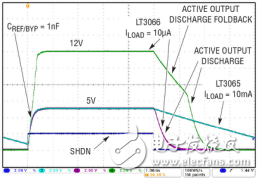
Figure 2: Comparison of the LT3066 with the LT3065 with active output discharge
ACTIVE OUTPUT DISCHARGE FOLDBACK: Active output discharge foldback
ACTIVE OUTPUT DISCHARGE: Active output discharge
The LT3065 has a 10mA load and the LT3066 is only loaded by a resistor divider that sets the output voltage (10μA in this example). Even if a very light load is applied to the output of the LT3066, the output voltage is quickly discharged because the device provides active output discharge. In contrast, the output capacitor of the LT3065 is only discharged by a 10mA load connected to it, and the discharge rate is much slower.
For output voltages above about 7V, the LT3066 implements active output discharge foldback, so the drive for the active output discharge is reduced, which limits the power consumed by the device. Due to the foldback, it is seen on the oscilloscope display that the LT3066's 12V waveform does not discharge as fast from 12V to 7V. This discharge rate protects the LT3066 from damage when the output voltage is high and large capacitors are used, or in the event of a fault, shorting the output to a very high voltage.
The main advantage of devices with active output discharge is that the outputs are in a set known state when the device is turned off. The output is always discharged as expected, regardless of the state of the load. This feature is important for applications that require precise power sequencing during shutdown.
PSRR performance improvementsCompared to other devices in the LT306x family, the LT3066 improves PSRR performance through the INFILT pin. The INFILT pin is a separate input that powers the error amplifier and reference. This pin is connected to the IN pin through an internal 140? resistor. By connecting a decoupling capacitor between the INFILT pin and ground, an RC filter is formed to reduce the input supply ripple of the error amplifier and reference. A 0.47μF decoupling capacitor is connected to the INFILT pin to improve the PSRR by up to 30dB at frequencies above 10kHz. If input filtering is not required, connect the INFILT pin to the IN pin. Figure 3 shows an improvement in the LT3066 PSRR performance compared to the LT3065.
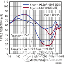
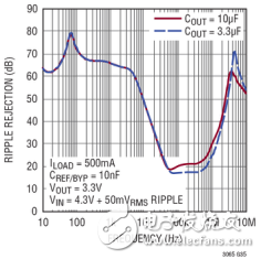
Figure 3: Comparison of the PSRR of the LT3066 with the INFILT pin and the LT3065
RIPPLE REJECTION: Ripple suppression
FREQUENCY: Frequency
Complete LT306x SeriesNot all applications require active output discharge to protect sensitive loads, and not all applications require output currents up to 500mA. As a result, Linear Technology has developed an additional five devices in the LT306x family to provide an attractive product portfolio with high input and output voltages, low dropout voltage, and low output voltage noise. Performance, extensive protection, fast response and a wide 100mA to 500mA output current. Some of these devices have an active output discharge function, and some devices do not. Table 1 below highlights the differences between the various devices in the LT306x family.
Table 1: LT306x Series LDO Features and Features at a Glance

New circuit design methods and improved chip fabrication processes enrich the performance characteristics of PNP-based transistor LDOs. These LDOs from suppliers such as Linear Technology offer reliable protection, a wide input and output voltage range, low output noise and fast response, and can operate with a single voltage source with low dropout. The new LT306x family has six devices with output currents ranging from 100mA to 500mA, and three of these devices offer a new complete dual-action active output discharge capability that is ideal for use in image sensors and high reliability systems. Protect sensitive, costly loads while achieving precise power sequencing.
Wholesale OEM Available 800 Puffs Electronic Cigarette Vape Disposable
This Elegant pre-filled disposable pod system with slim body featured with advantages as below:
1, Under Voltage Protection
2, 3.6V Constant Output
3, LED Light Battery Indicator
4, 10 Seconds Cut-Off Protection
5, Short-Circuit Protection
6, Over Temperature Protection
2ml energy fruit flavor e-juice, 450mAh battery build-in, small in size, let you enjoy amazing vaping experience on the go.
Flavors:
1. Fizzy Cola
2. Ice Grape
3. Ice Lychee
4. Ice Watermelon
5. Mango Butter
6. Mango Smoothie
7. Nutty Tobacco
8. Strawberry Milkshake
Electronic cigarette,e-cigarette,vapes e cigarette electronic,disposable vape,vape pen
Shenzhen Axiswell Technology Co., Ltd , https://www.medhealthycare.com