Sequential circuit designed using CPLD chip and digital control technology
The six-degree-of-freedom electromagnetically sensitive positioning system is a new type of tracking and positioning device that can determine the six parameters of the target in real time. It has been obtained in airborne fire control systems (helmet sights), precision medical devices, and individual combat simulation training. Widely used [1, 2]. The tracking system is composed of two parts, a sine signal transmitting circuit and a sensitive signal receiving circuit hardware and an algorithm program for solving target parameters from the sensitive receiving data. The positioning accuracy is subject to the errors of the above two parts. At present, without considering the influence of environmental factors, the algorithm error has reached the level of less than 1 milliarc. Therefore, the error of the hardware circuit becomes the main factor that restricts the positioning accuracy of the system. According to the principle of operation, the system uses the time-sequential excitation of the transmitting antenna so that the target parameters can be calculated based on the receiving matrix of the sensitive antenna. However, as the analog device of the timing control circuit, there are unavoidable temperature drift and time drift problems, which greatly affect the accuracy of the timing emission, and reduce the accuracy of the system positioning calculation. In order to solve this problem, this article uses CPLD digital control technology to improve the sequential circuit. CPLD (Complex Programmable Logic Device) is a new generation of digital logic devices, with features such as high speed, high integration, high reliability, user-reusable programming, or dynamic reconstruction of its logic functions. Using the sequential circuit designed by CPLD chip and digital control technology, the accuracy of the timing control can be improved to nanoseconds, and the operation is stable, free from the influence of temperature, which is beneficial to the improvement of the positioning accuracy of the system.
System principle
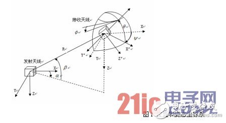
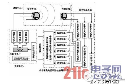
The working principle of the six-degree-of-freedom electromagnetic sensitive system [2] is as follows: Taking the three axes (x, y, z) of the transmitting antenna as the reference coordinate system, the position parameters of the receiving antenna relative to the transmitting antenna are represented by distance, azimuth and elevation angles. The attitude parameters are represented by the yaw angle, pitch angle, and roll angle. The six parameters are the target parameters to be calculated, ie six degrees of freedom, see FIG. The system consists of sine signal generator, timing control circuit, power amplifier circuit, three-axis loop antenna, receive signal amplification circuit, wave detection phase detection circuit, and data acquisition and parameter calculation circuit. Refer to Figure 2.
?
?
When the system is working, the transmitting circuit in turn stimulates the three-way loop antenna of the transmitting antenna in a time-division manner. Each time the excitation circuit receives three signals, the receiving antenna (three paths in total) receives a total of nine signals in a single excitation period. The signals, the receiving matrix consisting of nine signals, can calculate all the target parameters.
Timing control circuit design
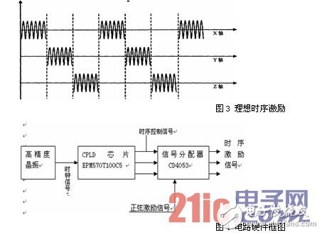
According to the working principle of the system, the three-way transmit antenna must be excited by the time division method. Therefore, the accuracy of the time sequence control is very important in improving the accuracy of the tracking and positioning of the system. However, due to the finite precision of the analog components used in the original sequential circuit and the analog components affected by the temperature, the timing control signal drifts and the precision is low, so that the actual value of the receiving matrix element is greatly deviated from the theoretical value. Affects the system's calculation accuracy. In order to improve the accuracy of the system positioning calculation, the accuracy of the system timing control must be improved. Based on this, this paper designs a new digital timing control circuit on the MAX II series chip EPM570T100C5 according to the CPLD digital control technology, which greatly improves the system timing. The accuracy of the control improves the accuracy of the system calculation. Circuit composition as shown in Figure 4.
?
The 32MHz high-precision crystal oscillator provides an accurate clock signal. The MAX II chip EPM570T100C5 generates accurate timing control signals. The EPM570 is a world-class, low-cost device suitable for implementing any digital control function. The chip uses a non-volatile single-chip solution that can solve board-level issues such as insufficient processor I/O pins, manage power-up sequencing, configure other more complex devices, or implement incompatible interfaces at low cost ("Glue logic" The conversion of "). With low cost, zero power consumption, small package, instant start and non-volatile, in-system programmability (ISP) and other advantages. The CD4053 completes the time-sequential excitation of the sinusoidal signal based on the precise timing digital control signal provided by the CPLD chip.
software design
In the CPLD development process, Quartus II, a CPLD development software provided by Altera Corporation, is used. This software supports most of Altera's devices. In order to shorten the design cycle and reduce the design complexity, QuartuslI includes functions such as workgroup computing, integrated logic analysis, EDA tool integration, multi-project support, enhanced recompilation, and IP integration. In the design process, the design concept from the top to the bottom is adopted, and the top layer is based on the design of functional blocks. The underlying specific functions are realized through VHDL programming.
Top-level design
The top-to-bottom design process begins with system-level functional design in software and then designs and validates different functional blocks in the system. The advantage of this design method is that it can continuously add new functional modules to the design and improve the system's functionality.
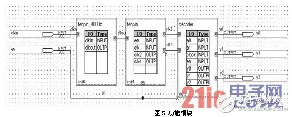
Three functional modules are mainly designed in the top layer: pre-divided modules, sub-divided modules, and decoding modules. The functional block diagram is shown in Figure 5. When the system is powered on, the crystal is first used to provide the system with an accurate baseband signal. The prescaler module converts the original baseband signal to a 400Hz timing signal, and the 400Hz signal is divided by a second frequency divider module. Quadrature frequency [6,7], the frequency demultiplied 100Hz and 200Hz signal enters the decoder module [7], through the decoding produces the accurate time sequence control signal which the time interval is 2.5ms.
?
Bottom design
After the system function verification is completed, the abstract top-level design is refined to the low-level design. The bottom software design is based on the top three major functional modules. The module design is completed using VHDL language, and the bottom layer is compiled, synthesized and simulated. Design files for top-level design calls. Take the fenpin module as an example, part of the program is as follows:
Architecture rt of fenpin is
Signal temp :std_logic_vector(1 downto 0);
Begin
Process(clk,temp,en)
Begin
If en='1' then
If rising_edge(clk) then
Temp<=temp+'1';
End if;
Null;
End if;
End process;
Clk2<=temp(0);
Clk4<=temp(1);
End rt;
System Simulation and Verification
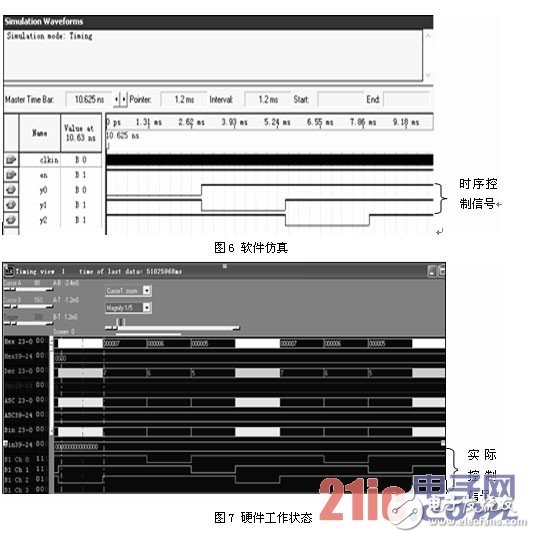
After the software design is completed, specify the chip as EPM570T100C5 by the Quartus II software, and perform pin assignment according to the circuit schematic, set the pin function of the CPLD, and then start the compiler to compile the project. The compiler will perform error checking, netlist extraction, logic synthesis, and device adaptation. It will then perform behavioral simulations, functional simulations, and timing simulations. Finally, the file will be downloaded to the chip via JTAG programming using a download cable to generate the hardware circuitry.
Figure 6 shows the simulation result of the system software. It can be seen from the figure that the generated timing control signal is stable and the accuracy is nanoseconds.
Figure 7 shows the actual working state of the system when the program is downloaded to the target chip and the hardware is working through the logic analyzer. It can be found that the actual working state of the system is consistent with the theoretical design concept. The three-way sequential control signal in the figure has high precision, stable state, no glitch and drift, and lays the foundation for improving the stability of the system and the accuracy of the receiving matrix.
Optical Rotary Sensor,Custom Encoder,Optical Encoder 6Mm Shaft,Handwheel Pulse Generator
Jilin Lander Intelligent Technology Co., Ltd , https://www.jllandertech.com