ADA4896: ADI Rail-to-Rail Output Amplifier
The ADA4896-2/ADA4897-1/ADA4897-2 are unity-gain stable, low noise, rail-to-rail outputs, high speed voltage feedback amplifiers with quiescent current of 3 mA and 1/f noise of 2.4 nV/_Hz (10 Hz). With a spurious-free dynamic range of −80 dBc (2 MHz), it is an ideal solution for a wide range of applications including ultrasound, low noise preamplifiers and high performance ADC drivers. ADI's proprietary next-generation SiGe bipolar process and innovative architecture create such a high performance amplifier.
Typical performance value
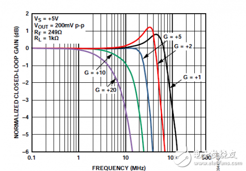
To reduce design time and eliminate uncertainty, Table 1 provides reference values ​​for typical gain, component values, and performance parameters. The power supply voltage used is 5 V. The bandwidth is obtained at a small signal output of 200 mV pp and the slew rate is obtained at a 2 V output step. Note that as the gain increases, the small signal bandwidth decreases, which is consistent with the gain-bandwidth product. In addition, the higher the gain, the larger the phase margin, and the more stable the amplifier becomes. Therefore, the peaking of the frequency response is reduced (see Figure 1).
Table I:


Figure 1. Small signal frequency response at different gains
Low noise gain optional amplifier

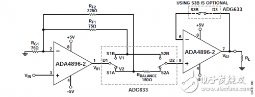
Figure 2 uses the ADA4896-2 and ADG633 to build a low noise gain selectable amplifier to drive a low resistive load.
The gain selectable amplifier supports the processing of a variety of different input signals. A conventional gain-selectable amplifier uses a switch in the feedback loop to connect the inverting input. Switching resistors reduce the noise performance of the amplifier and add a large amount of capacitance to the inverting input node. Noise and capacitance issues are especially troublesome when using low noise amplifiers. In addition, switching resistance can also cause annoying nonlinear gain errors. Figure 2 shows an innovative switching technique used in a gain-selectable amplifier that maintains the 1 nV/Hz noise performance of the ADA4896-2 while greatly reducing nonlinear gain errors. With this technology, the user can also choose the switch with the smallest capacitance to optimize the bandwidth of the circuit. In the circuit shown in Figure 2, the switch is implemented using the ADG633, configured with S1A and S2A turned on, or S1B and S2B turned on.
In this example, when switches S1A and S2A are turned on, the first stage amplifier gain is +4; when switches S1B and S2B are turned on, the first stage amplifier gain is +2. The first set of switches of the ADG633 is placed at the output of the feedback loop, and the second set of switches is used to sample at a point (V1 or V2) where the switching resistance and the non-linear resistance are not critical. This reduces gain error while maintaining the noise performance of the ADA4896-2.
Note that the input bias current of the output buffer is a circuit error with the impedance of the sampling switches S2A and S2B. The relationship between these two sampling switches and voltage and temperature is nonlinear. If this is a problem, the unused switch (S3B) of the ADG633 should be placed in the feedback path of the output buffer to balance the bias current (see Figure 2). In addition, the bias current of the input amplifier causes an offset at the output that varies with the gain setting.
Since both the input amplifier and the output buffer are single-chip devices, the relative offset of their bias currents can be utilized to eliminate these offset variations. A more stable offset voltage can be obtained by connecting a resistor of the same magnitude as RF2 to RF1 in series with switch S2A. The following derivation formula shows that sampling at V1 produces the required signal gain with no gain error. RS represents the switching resistance. V2 can be derived using the same method.
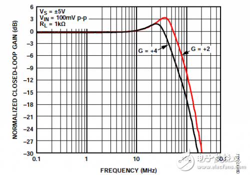
Equation 1 Note that if V01 produces the desired signal gain and no gain error, the buffered output V02 also has no gain error. Figure 3 shows the normalized frequency response of the circuit at V02.

Figure 3 Frequency response of V02/VIN
Medical ultrasound application diagram ultrasound system overview

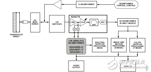
Figure 4 is a simplified functional block diagram of the ultrasound system
Medical ultrasound systems are among the most complex signal processing systems in use today. The ultrasound system can generate images of internal organs and structures, generate blood flow and tissue motion maps, and provide highly accurate blood flow velocity information by emitting acoustic energy to the human body and then receiving and processing the echoes. Figure 4 shows a simplified functional block diagram of an ultrasound system.
The ultrasound system mainly includes two operations: time gain control (TGC) operation and continuous wave (CW) Doppler operation. The AD9279 integrates the key components of these two operations into one IC with an 8-channel variable gain amplifier (VGA), a low noise preamplifier (LNA), an anti-aliasing filter (AAF), and an analog-to-digital converter. (ADC) and I/Q demodulator with programmable phase rotation. See the AD9279 data sheet for details on how to use the AD9279 in an ultrasound system.
In ultrasound applications, the ADA4896-2/ADA4897-1/ADA4897-2 are used in the continuous wave Doppler path after the AD9279 I/Q demodulator. The Doppler signal is typically in the range of 100 Hz to 100 kHz. The low noise floor and high dynamic range of the ADA4896-2/ADA4897-1/ADA4897-2 make it an excellent choice for handling weak Doppler signals.
The ADA4896-2/ADA4897-1/ADA4897-2 offer rail-to-rail output and high output current drive, making them ideal for current-to-voltage converters, current adders, and ADC drivers. Figure 4 shows the interconnection block diagram for all eight channels of the AD9279. Use two stages of the amplifier ADA4896-2. The first stage performs current-to-voltage conversion and filters the high-frequency components generated by the demodulation process. The second stage is used to summarize the output current of multiple AD9279 devices to provide gain and drive the AD7982 18-bit SAR ADC. The reduced-to-output noise of the CW signal path depends on the LNA gain, the choice of the first stage summing amplifier, and the RFILT value. To determine the noise to the output, you must know the RA, RFILT, and CFILT values ​​of the active low-pass filter (LPF).
Typical filter values ​​for all eight channels of a single AD9279 are: RA is 100 _, RFILT is 500 _, and CFILT is 2.0 nF; a 100 kHz single-pole low-pass filter is now available. By increasing the filter resistance RFILT, the gain of the current-to-voltage converter can be increased. In order to keep the corner frequency constant, the filter capacitor CFILT should be reduced by the same ratio. The factors that limit the gain amplitude are the output swing and the load drive capability of the current-to-voltage converter (in this case, the ADA4896-2/ADA4897-1/ADA4897-2). Any amplifier has limited drive capability and can only drive a limited number of channels.
Telecom systems is the exchange of information over significant distances by electronic means. A complete, single telecommunications circuit consists of two stations, each equipped with a transmitter and a receiver. And we will offer the basic telecom products which you may familiar in your life to build up the telecom systems.
From Data center with a floor standing cabinets, you may get your sign out .For distribution outdoor, you may need a waterproof Distribution Box to exchange the singals. Meanwhile, you may have a terminal block with 10 pair disconnection Krone Module and lighting protectors(LSA single pair type or STB module). When you distribute in house, there are more products in application like voice patch panels, keystone jacks, face plate, 3M connectors(like UY connectors), AMP picapond connector, wall outlets, surface mount box, and so on. Sure there is a must to get the right tool to finish operations, kinds of tools for selection: Insertion tools, punch tool, crimping tool, wire cutter, cable stripper. Hot sale for krone insertion tool, RJ45 crimping tools, Ericsson punch down tool, AMP picabond ratechet crimper, Coaxial cable crimping tool .
We insist on compact size to ensure an easy but smart and reliable installation in every product of the telecom systems we offer. That is the final aim we work on solution, to make it perfect we also provide OEM service to satisfy your special demand. Till now, we have successfully take part in many Telecom projects in Russia, Sri Lanka, Greece, Ecuador, ect.. We have full experience in such tenders for building up telecom systems.
We keep on working just like the Cable Ring Managers to keep everything Orderly, Fast and Effective. Believe us and we will help you to be the winner !

Outdoor Distribution Box, LSA Krone Module, Mounting Frame, STB Module, Picabond Connector , Crimping Tool
NINGBO YULIANG TELECOM MUNICATIONS EQUIPMENT CO.,LTD. , https://www.yltelecom.com