Analysis of the principle of micro motor drive circuit
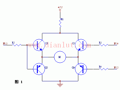
As shown in Figure 1, this circuit is the circuit originally designed by the author. P1.3, P2.2 and P2.4 are the IO pins of the 51 MCU, respectively. The working principle of the design is: When P1.3 high level, P2.2 and P2.4 are both low level, the motor rotates forward. At this time, Q1 and Q4 are turned on, Q2 and Q3 are turned off, and the current direction is +5VÃ R1Ã Q1Ã MÃ Q4; when P1.3 low level, P2.2 and P2.4 are both high level, the motor is reversed. At this time, Q2 and Q3 are turned on, and Q1 and Q4 are turned off. When P2.2 is high and P2.4 is low, the circuit is completely disabled and the motor stops.
In the figure, the resistance is: R1=20Ω, R2=R3=R4=510Ω, but the actual experimental situation is unexpected, that is, the motor does not rotate in the forward and reverse directions. After measurement, when P1.3 is high, P2.2 and P2.4 are both low, Q4 is turned on, but Q1 is not turned on, and the level of P1.3 is only about 0.67V, so Q1 cannot be turned on. .
The reasons for analysis are as follows: 51 P1, P2, P3 pins are internally pulled through the resistor, connected to the ground MOSFET, the so-called high level, is the MOSFET cut-off, the pin pull-up resistor is pulled high. If the internal pull-up resistor is large, such as 20K, then when the circuit above is connected, the current flowing through the b-pole of Q1 is (5-0.7)/20mA=0.22mA, which is difficult to turn on. Therefore, this circuit does not work.
Summary: The pin pull-up capability of the 51 MCU is weak, which is not enough to drive the triode to conduct.
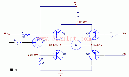
As shown in Figure 2: The four transistors in this circuit are PNP type, so that the conduction drive is the control pin output low level, while the 51 low level is through the MOSFET ground, so the pull-down capability is very strong.
However, Q1 and Q3 of this circuit need to be separately controlled, and more control pins are required. If you want to use an IO pin control, you can add an inverter. However, Q1 and Q3 of this circuit need to be separately controlled, and more control pins are required. If you want to use an IO pin control, you can add an inverter. As shown in Figure 3. The measured voltage values ​​at each point are marked in the figure.
In circuit 2, since the emitters of Q2 and Q4 are 0.7V higher than the base and the base is 0V, the emitter of Q2 and Q4 is not lower than the actual MOSFET tube voltage drop inside the CPU pin. 1V, this reduces the effective voltage range across M.
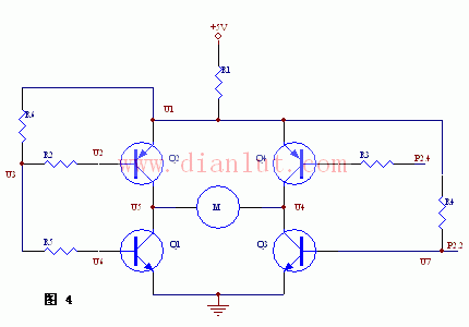
To solve this problem, Q2 and Q4 need to be replaced with NPN tubes. However, the driving of the NPN tube is as shown in circuit 1. It is not possible to pull up the CPU pin only, so it is necessary to add a pull-up resistor, as shown in Figure 4.
In Figure 4, unlike the circuit one, the two NPN tubes are moved below and the PNP is above, so that the potential of the collectors of Q1 and Q3 can reach a tube drop (0.3V). This increases the pressure drop range of M.
However, in order to ensure sufficient driving of the NPN tube, P1.3 and P2.2 must be added with pull-up resistors, as shown in Figure 4. In the figure, R2, R5, and R6 are indispensable. Therefore, the components of this circuit are used in a relatively large amount.
Also, R5 should be several times larger than R6, such as 10 times. Thus, when Q1 is turned on, the voltage at P1.3 can be divided to be large, so that Q2 is not turned on. If R5 is too small or 0, then when Q1 is turned on, since the voltage drop at P1.3 is only about 0.7V, Q2 will also be turned on.
After testing, R2, R6, R3, R4 can take 510Ω, and R5 takes 5.1kΩ. The voltages at this value are as follows (R1 is 20 ohms):
U1:4.04 U2:2.99 U3:3.87 U4:4.00 U5:0.06 U7:
This circuit is modified from the circuit, as shown in Figure 5 below, with the measured voltage values ​​at each point:
The current-limiting resistors in this figure are removed because the circuit designed by the author requires less components. From the circuit analysis, don't matter, R1 plays the role of total current limiting, and there is a pull-up resistor inside the pin, so that the circuit will not pass too much current.
This circuit allows the motor to run.
However, in the choice of R2, it is more stressful, because the pull-up effect of R2 not only has an effect on Q1, but also on the conduction of Q2. If R2 is selected too small, although it is favorable for the conduction of Q1, it is effective for the conduction of Q2, because the smaller the R2 is, the stronger the pull-up effect is, and the conduction of Q2 is the higher the P1.3 potential. The lower the better, so this is contradictory. That is to say, the conduction condition of Q1 and the conduction condition of Q2 are contradictory.
After experiment, R2 is suitable for 5.1k ohms. It can be seen that although this circuit saves components and CPU pins, the driving capability has a maximum limit. That is, the driving of Q1 and Q2 is mutually constrained, and only a compromise solution is obtained. Otherwise, if one magnification is large, the other will become smaller.
Summary: The above circuits are all beneficial, depending on the application field.

What Is Adapters And Converter
An Adapter object acts as a bridge between an AdapterView and the underlying data for that view. The Adapter provides access to the data items. The Adapter is also responsible for making a View for each item in the data set.Basically all that adapter does is that it allows you to plug your current device into another plug for example.

iphone adapter,vga to hdmi adapter,displayport to hdmi adapter,hdmi to vga adapter,usb adapter
Pogo Technology International Ltd , https://www.wisesir.net