Use modular architecture application processor to expand mobile phone functions
Use modular architecture application processor to expand mobile phone functions
In the next generation of multi-functional mobile phones, applications such as DSC, MP3, games and video are in full bloom. If only the baseband chip is used to realize these functions, it will significantly increase the CPU load and affect the communication processing performance. The application processor (AP) is suitable for expanding the functions of mobile phones, and the AP subsystem with a modular architecture can be reused in mobile phones of different mobile system formats. This article will discuss the requirements for APs and the integration of APs with existing baseband chips.
Most mobile phone manufacturers will use the reference design solutions provided by semiconductor suppliers. This scheme is mainly composed of object code and a small amount of source code. It is difficult for R & D engineers to modify the scheme and add new functions. In addition, the limited resources of the baseband chip make it impossible to implement high-load multimedia applications, such as DSC, MP3, MPEG-4, games, and video phones, which are necessary for high-end mobile phones.
These manufacturers are experienced in the hardware and software of the reference solution. The quality of the reference scheme has been verified and proven in commercial products. It's better to reuse it in subsequent products instead of re-developing all functions. In order to upgrade existing mobile phone designs to high-end phones, the application processor architecture is a shortcut for manufacturers. The existing baseband system can be reused and connected to an AP subsystem. The subsystem is similar to a module and can be connected to a baseband system.
The traditional method of modular architecture to extend the characteristics of mobile phones is to write and execute new applications on the baseband chip. This single-chip architecture requires engineers to upgrade the baseband chip to obtain more CPU power. In order to realize the connection of the camera function and SD / MMC, the circuit must be redesigned. The baseband code should be transplanted into the new chip. Existing functions must be thoroughly re-verified, even if they have been tested before. In addition, for this single-chip architecture, the size of the program code will be very large and very complex. This leads to longer development and debugging time, and ultimately increases the cost of development.
By adopting a modular AP architecture, multimedia function applications that used to consume too much CPU resources can be executed on the AP. Most of the codes and circuits on existing mobile phones can be reused with only a slight modification. Software engineers can therefore focus on developing new applications. These applications only need to be developed and debugged on the AP.
This dual-processor solution separates baseband work from AP work, with one processor implementing basic telephony functions and the other processor implementing multimedia functions. The baseband processor implements basic phone functions such as call / answer made by current mobile phones, and the AP processor is dedicated to handling high-load multimedia applications. This eliminates the risk of baseband failure caused by newly applied software defects. For example, an unpaired disable / enable interrupt on a new application will suspend the real-time operating system schedule, which will terminate all telephony functions if it is executed on a single processor.
The communication between the baseband and the AP processor is realized by message passing. The command to activate or deactivate the new application is transferred from the baseband processor to the AP processor in the format of a message.

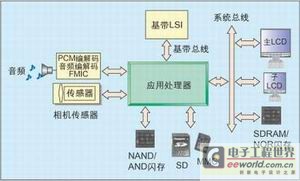
In the form of a modular architecture, the AP constitutes a subsystem and is isolated from the baseband processor. The main LCD and sub-LCD are connected to the AP instead of the baseband processor in order to achieve the best visual performance for multimedia applications. The audio encoder / decoder can be connected to the baseband or AP processor, depending on the difficulty involved. The video I / O hardware on the AP is dedicated to the camera sensor. It decodes the camera output in YUV format and converts it to RGB for display. The SD / MMC card is connected to the AP to store data externally. On-chip NAND / AND flash memory can be used to store data and main programs other than the boot loader. NOR flash memory can also be used to store the main program and boot loader, depending on cost. SDRAM is used as running memory. For multimedia applications that process image data, it should be large. The AP subsystem is shown in Figure 1.

AP subsystem requirements Simple connection AP must be easy to connect to the baseband processor. The easiest way to connect is to use an SRAM interface. It can be flexibly connected to 8-bit and 16-bit bus baseband systems. In addition, it needs to be compatible with 8086 and 68000 system buses. The SRAM interface bus is isolated from the AP system bus so that the baseband access AP bus and the AP access system bus can work simultaneously.
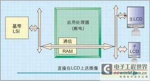
2. The "pass through" feature is because the LCD is connected to the AP instead of the baseband processor, so extracting the image from the baseband and sending it to the LCD becomes an indirect action. The traditional fetch method requires two steps: the first step is to send a fetch command from the baseband to the AP; the second step is to send image data from the AP to the LCD. In this way, the AP should be in the power-on state, thus increasing power consumption. And the existing baseband code should be modified based on the direct access command. Engineers need time to develop, test and correct errors.
The "pass through" feature on the AP processor allows the baseband processor to access the LCD even when the AP is in power saving mode (see Figure 2). In this mode, both the main LCD and the sub LCD can be accessed. The maximum number of devices that can be "passed through" is set to 4. This reserves space for future expansion. The power consumption is the lowest in the power saving state. Therefore, the standby time of the mobile phone can be maximized. With this direct access feature, existing code can be reused without modification. It reduces the workload of engineers and shortens development time.
3. Baseband boot function Normally, NOR flash memory is used to store AP programs. It can be removed when the AP provides the function of receiving the boot code, that is, the AP receives the boot code (boot loader) from the baseband processor and then runs the code. By taking advantage of this feature, the main program can be stored on inexpensive NAND / AND flash memory. The boot loader loads the main program from the data flash to SDRAM, and finally runs it on the SDRAM. A different bootloader can be used to rewrite / update the main program. Even if an abnormal interruption occurs during rewriting, there is no damage to the final product. This is because the rewritten boot loader is stored on the baseband instead of the AP's flash memory.
4. Video I / O
The video interface hardware on the AP is dedicated to decoding the output signal of the camera sensor. It does not need to write code to detect the horizontal and vertical signals from the sensor, and decodes it into row and column data. Converting YUV to RGB or RGB to YUV is achieved by hardware, not software calculation. This brings speed and efficiency. The output YUV format of an SXGA resolution camera sensor is 4: 2: 2, 15 frames per second, which means that 1,280 × 1,024 × 8 × 15 = 157,286,400 bytes can be processed per second. If you rely on software to calculate, this will consume a lot of CPU resources.

5. Integrated baseband and AP
The integration of the baseband system and the AP subsystem is similar to adding an SRAM to the baseband processor. The baseband should reserve up to 7 I / O ports and an interrupt to control the AP. The removal of certain AP functions, such as "baseband guidance" and "pass through", can reduce the demand for I / O.
This article summarizes the various applications on mobile phones will increase the complexity. It is difficult or even impossible for these applications to be fully implemented by the baseband processor. Application processor architecture simplifies the work of engineers, they can extend the existing mobile phone design to the next generation of multimedia phones. This modular architecture minimizes modifications to existing mobile phone design solutions, allowing engineers to concentrate on developing new applications. It also allows engineers to develop and debug applications on the baseband and AP separately, significantly reducing development time. By using different basebands, this architecture allows handset manufacturers to reuse the hardware and software on the AP subsystem for different mobile systems.
BLPS laser safety protective device is designed for personal safety used on hydraulic bender.
The dynamic test technology it used has passed the Type 4 functional safety assessment by TUV, and get the national invention patent. The product reaches the advanced technological level of similar products.
BLPS laser safety device provides protection zone near the die tip of the bender to protect fingers and arms of the operator in close to the upper mold die tip. It is the most effective solution so far to preserves the safety and productivity of the bender.
Press Brake Protection,Laser Safety Guard Device,Laser Guarding Device,Press Brake Laser Guard,Press Brake Guarding Systems,Press Brake Guarding
Jining KeLi Photoelectronic Industrial Co.,Ltd , https://www.sdkelien.com