AD9522 clock frequency division circuit schematic
In today's highly developed integration, it is impossible to solve the problem by multiple crystal sources, and once the crystal is fixed, its flexibility and portability will be greatly affected, so some clock crossover chips have emerged. Today we will A typical application of the representative AD9522 clock crossover chip is used to achieve a role.
1. Introduction to AD9522 1. External Features AD 9 5 2 2 is a multi-channel clock output and distribution function chip that supports sub-picosecond jitter performance. It also integrates PLL (PhaseLockedLoop) and VCO (voltage controlled oscillator) inside the chip. ). The tuning range of the VCO is 2.02GHz~2.335 GHz. The AD9522 serial interface supports the data bus of SPI and I2C. The internal EEPROM of the chip can be programmed through the serial port, which can be used to store the user-configured register data to divide the input clock. The AD9522 has 12 channels of LVDS level output, which can be divided into 4 groups. Each group has a frequency divider. The division ratio can be set freely within the range of 1-32. As shown in Figure 1. 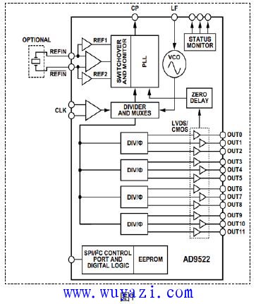
2. Internal Characteristics The external input clock of the AD9522 is supplied by the crystal oscillator. The multiplication and division of the internal clock are controlled by the phase-locked loop PLL and the voltage-controlled oscillator VCO. For example, the voltage controlled oscillator gives a signal, one part is used as the output, and the other part is phase-compared with the local oscillator signal generated by the PLL. In order to keep the frequency constant, the phase difference is not changed, if there is a phase difference change. Then, the voltage at the voltage output end of the PLL changes, and the VCO is controlled until the phase difference is restored to achieve the purpose of frequency locking. As shown in Figure 2. 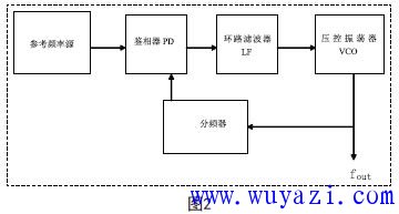
Second, the microcontroller configuration 1. Register configuration We mentioned that the AD9522 can configure the data bus of SPI and I2C to achieve the purpose of frequency division, then the configuration data bus can be configured with a single chip. We chose C8051F320 as the internal register of AD9522, because the programming of MCU is relatively intuitive and easy. As shown in Figure 3. 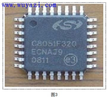
After the completion of the write, set the breakpoint to observe whether the write and read values ​​are the same, and verify that there is no problem after reading the configuration register. When configuring, note that the 0×18 address register configuration lock detection period number is larger. It is possible that some setting parameters or loop filter bandwidth settings result in a longer lock time, resulting in a lock status when reading 0 x 1 F address. In the final state, set this register to 0x66 and set the number of detection cycles to the maximum value of 255.
The VCO check needs to first set 0×18 to 0 and then update, and then set 0×18 to 1 to update again. Wait for the verification to finish reading the 0x1F address data. 0x1D needs to be set to 0, and the Status pin shows the status as 0 x 1 7 address configuration status. Otherwise the derived clock is not observed. After the configuration is complete, the 0x1f address status is read. After the configuration is complete, it takes a certain period of time to read the 0x1f address data. Because the vco check takes a certain amount of time, reading too fast will result in incorrect read status.
As shown in Figure 4, the VCP needs to be pulled up on the pin pull-down. PD, SYNC, and RESET need to be pulled up to disable these pins. The EEPROM causes the internal register values ​​not to be loaded from the EPROM. SP1, SP0 need to be pulled down, set the internal register data loading configuration mode to I2C loading. The CS pull-down causes the data chip select signal to remain valid. REF_SEL pulldown selects the input reference clock as refrence1. 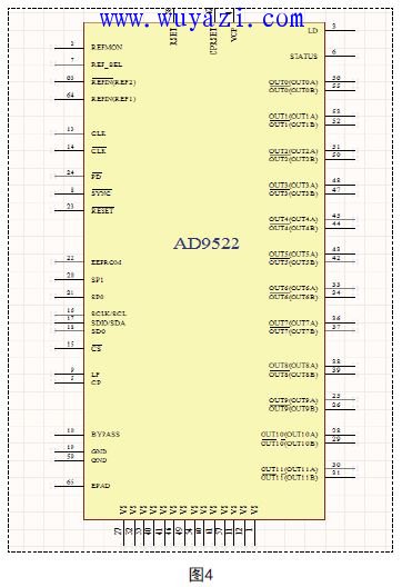
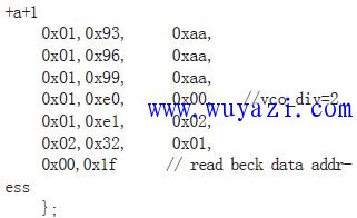
2. Program design MCU source program register configuration part mainly configures the values ​​of a, b, p, div and vco div, then we can determine the value of fvco according to the formula fvco=ref*(a+b*p), then according to us The frequency divider formula fout=fvco/vco div/div gives us the clock frequency we need. The register configuration part of the program is as follows: 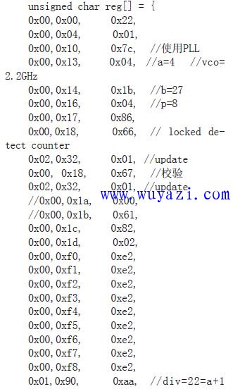
Third, loop filter design So we have to mention that the loop filter parameter setting of AD9522 must be consistent with the above register configuration, so that we can lock the frequency, so that the clock frequency we divide is stable and we need Clock frequency. Setting loop filtering can be handled with the ADIsimCLK software. As shown in Figure 5. 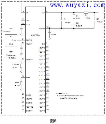
IV. Conclusion After the above discussion, we can conclude that the AD9522 is a very useful crossover chip. It can get 12 channels of clocks we need according to the input clock we give, internal frequency locking, multiplier and frequency division. The frequency can be said to be extremely convenient for design. It can provide more clock sources for us to use in subsequent designs. The configuration of its registers is where we learn and learn. (Author: Jia Zhen'an, Yang Xiaojing)
Bi Directions Thyristor (Triac)
Bi Directions Thyristor (Triac) is equivalent to the antiparallel connection of two unidirectional thyristors, but only one control pole.
Bidirectional thyristors are made of N-P-N-P-N five-layer semiconductor materials, and three electrodes are also derived from the outside. Its structure is shown in the figure. Bi-directional thyristor volt-ampere characteristic curve Since the forward and reverse characteristics of the bidirectional thyristor are symmetrical, it can be turned on in any direction and is an ideal AC switching device.
Bi Directions Thyristor,Electronic Components Triac,Power Thyristor For Inverter,Silicon Power Bipolar Transistors
YANGZHOU POSITIONING TECH CO., LTD. , https://www.cnchipmicro.com