Application know-how and skills of using LVDS in high-speed data converter implementation
The interface of field programmable gate array (FPGA) and analog-to-digital converter (ADC) output is a common engineering design challenge. This article briefly introduces various interface protocols and standards, and provides application tips and techniques for using LVDS in high-speed data converter implementations.
The interface method and standard field programmable gate array (FPGA) and analog-to-digital converter (ADC) digital data output interface is a common engineering design challenge. In addition, ADCs use a variety of digital data formats and standards, making this challenge even more complicated. For low-speed data interfaces usually below 200 MHz, single data rate (SDR) CMOS is very common: the transmitter transmits data on one clock edge, and the receiver receives data on the other clock edge. This way can ensure that the data has enough time to complete the establishment, and then sampled by the receiver. In double data rate (DDR) CMOS, the transmitter transmits data on every clock edge. Therefore, in the same time, the amount of data it transmits is twice that of SDR. However, the timing of correct sampling by the receiver is more complicated.
Parallel low-voltage differential signaling (LVDS) is a common standard for high-speed data converters. It uses differential signals, and each bit has P and N lines; in the latest FPGA, its speed can reach DDR 1.6 Gbps or 800 MHz. The power consumption of parallel LVDS is lower than that of CMOS, but the number of lines required is twice that of CMOS, so wiring may be more difficult.
LVDS is often used in data converters with a "source synchronous" clock system, but this is not part of the LVDS standard. In this setup, the clock is in phase with the data and is sent with the data. In this way, the receiver can use the clock to capture data more easily because it now knows when the data transfer occurs.
The speed of FPGA logic generally cannot keep up with the bus speed of high-speed converters, so most FPGAs have a serializer/deserializer (SERDES) module to convert the fast, narrowband serial interface on the converter side to the slow speed on the FPGA side , Broadband parallel interface. For each data bit in the bus, this module outputs 2, 4, or 8 bits, but at a clock rate of ½, ¼, or 1/8 to effectively deserialize the data. The data is processed by the wide bus inside the FPGA, which is much slower than the narrow bus connected to the converter.
LVDS signal standards are also used in serial links, most of which are used in high-speed ADCs. When the number of pins is more important than interface speed, serial LVDS is usually used. Two clocks are often used: data rate clock and frame clock. All the considerations mentioned in the parallel LVDS section also apply to serial LVDS. Parallel LVDS is just composed of multiple serial LVDS lines.
I2C uses two wires: clock and data. It supports a large number of devices on the bus without additional pins. I2C is relatively slow, considering the protocol overhead, the speed is 400 kHz to 1 MHz. It is usually used on slow, small size devices. I2C is also often used as a control interface or data interface.
SPI uses 3 to 4 wires:
clock
Data input and data output (4-wire), or bidirectional data input/data output (3-wire)
Chip select (each non-host device uses one line)
SPI can support as many devices as there are available chip select lines. It can reach a speed of about 100 MHz and is usually used as a control interface and data interface.
Serial PORT (SPORT) is a CMOS-based bidirectional interface that uses one or two data pins in each direction. For non-%8 resolution, its adjustable word length can improve efficiency. SPORT supports time domain multiplexing (TDM) and is usually used in audio/media converters and high-channel number converters. It provides approximately 100 MHz performance per pin.
Blackn processor supports SPORT, and SPORT can be implemented directly on FPGA. SPORT is generally only used for data transmission, but control characters can also be inserted.
JESD204 is a JEDEC standard for high-speed serial links between a single host (such as FPGA or ASIC, etc.) and one or more data converters. The latest specifications provide speeds up to 3.125 Gbps per channel or per differential pair. Future versions may provide 6.25 Gbps and higher speeds. The channel uses 8B/10B encoding, so the effective bandwidth of the channel is reduced to 80% of the theoretical value. The clock is embedded in the data stream, so there is no additional clock signal. Multiple channels can be combined to improve throughput, and the data link layer protocol ensures data integrity. In FPGA/ASIC, to realize data frame transmission, JESD204 requires far more resources than simple LVDS or CMOS. It significantly reduces the wiring requirements, but requires the use of more expensive FPGAs and PCB wiring is more complicated.

It is generally recommended that the following general suggestions are helpful when designing the interface between ADC and FPGA.
Use the external resistance termination of the receiver, FPGA or ASIC instead of the internal termination of the FPGA, so as to avoid mismatches causing reflections and exceeding the timing budget.
If the system uses multiple ADCs, do not use a certain DCO of a certain ADC.
When laying out the digital traces connected to the receiver, do not use a lot of "tromboning" to make all traces
Keep it the same length.
Use the series termination of the CMOS output to reduce the edge rate and limit the switching noise. Confirm that the data format used (twos complement or offset binary) is correct.
When using a single-ended CMOS digital signal, the logic level moves at a speed of approximately 1 V/nS, the typical output load is 10 pF (maximum), and the typical charging current is 10 mA/bit. The capacitive load as small as possible should be used to minimize the charging current. This can be achieved by driving only one gate with the shortest possible trace, preferably without any vias. Using damping resistors at the digital output and input can also minimize the charging current.
The time constant of the damping resistor and capacitive load should be approximately 10% of the sampling rate period. If the clock rate is 100 MHz and the load is 10 pF, the time constant should be 10% of 10 nS, or 1 nS. In this case, R should be 100 Ω. To obtain the best signal-to-noise ratio (SNR) performance, 1.8 V DRVDD is better than 3.3 V DRVDD. However, when driving large capacitive loads, SNR performance will degrade. The CMOS output supports a sampling clock rate of up to approximately 200 MHz. If driving two output loads, or if the trace length is greater than 1 or 2 inches, a buffer is recommended.

The ADC digital output should be treated with care, because transient currents may be coupled back to the analog input, leading to increased noise and distortion of the ADC.
The typical CMOS driver shown in Figure 2 can generate large transient currents, especially when driving capacitive loads. For CMOS data output ADCs, special measures must be taken to minimize these currents so as not to generate additional noise and distortion in the ADC.
Typical example

Figure 3 shows a 16-bit parallel CMOS output ADC. Each output has a 10pF load to simulate a gate load plus PCB parasitic capacitance; when driving a 10 pF load, each driver generates a 10 mA charging current. Therefore, the total transient current of this 16-bit ADC may be as high as 16 × 10 mA = 160 mA. Adding a small series resistor R at each data output end can suppress these transient currents. The value of this resistor should be appropriately selected so that the RC time constant is less than 10% of the total sampling period. If fs = 100 MSPS, RC should be less than 1 ns. C = 10 pF, so the optimal R value is about 100 Ω. Choosing a larger R value may reduce the output data settling time performance and interfere with normal data capture. The capacitive load at the output of the CMOS ADC should be limited to a single gate load, usually an external data capture register. Under no circumstances should the data output end be directly connected to the high-noise data bus. An intermediate buffer register must be used to minimize the direct load on the ADC output end.

Figure 4 shows a standard LVDS driver in CMOS. The nominal current is 3.5 mA and the common mode voltage is 1.2 V. Therefore, when driving a 100 Ω differential termination resistor, the swing of each input of the receiver is 350 mV pp, which is equivalent to a differential swing of 700 mV pp. These values ​​are derived from the LVDS specification.

There are two LVDS standards: one is made by ANSI and the other is made by IEEE. Although the two standards are similar and roughly compatible, they are not exactly the same. Figure 5 compares the eye diagrams and jitter histograms of these two standards. The IEEE standard LVDS swing is 200 mV pp, which is lower than the ANSI standard 320 mV pp, which helps to save the power consumption of the digital output. Therefore, if the IEEE standard supports the target application and connection with the receiver, it is recommended to use the IEEE standard.

Figure 6 compares the ANSI and IEEE LVDS standards when the trace length exceeds 12 inches or 30 cm. In both figures, the drive current adopts the ANSI version standard. In the figure on the right, the output current is doubled, which can purify the eye diagram and improve the jitter histogram.
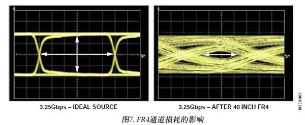
Figure 7 shows the effect of long traces on FR4 materials. The image on the left shows the ideal eye diagram at the transmitter. At the receiver end 40 inches away, the eye diagram is almost closed, and it is difficult for the receiver to recover data.
Troubleshooting tips ADC loses 14th position

In Figure 8, the VisualAnalog digital display of the data bit shows that the 14th bit has never changed. This may indicate a problem with the device, PCB, or receiver, or the unsigned data is not large enough to make the most significant bit jump.
Frequency domain curve when ADC loses the 14th bit

Figure 9 shows a frequency domain view of the above-mentioned digital data (where the 14th bit is not hopped). The figure shows that the 14th bit is meaningful and an error occurred somewhere in the system.
Time domain curve when ADC loses the 14th bit

Figure 10 shows the time domain curve of the same data. It is not a smooth sine wave, the data is offset, and there are obvious spikes at multiple points in the waveform.
The 9th and 10th bits of the ADC are shorted together

Figure 11 shows that one bit is no longer missing, but two bits are shorted together. Therefore, for these two pins, the receiver always receives the same data.
Frequency domain curve when ADC bit 9 and bit 10 are shorted together

Figure 12 shows the frequency domain view when the two bits are shorted together. Although the fundamental tone is very clear, the noise floor is significantly lower than expected. The degree of noise floor distortion depends on which two bits are shorted.
Time-domain curve when ADC bit 9 and bit 10 are shorted together
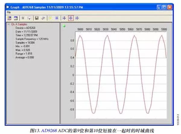
In the time domain diagram shown in Figure 13, the problem is relatively unobvious. Although some smoothness is lost at the peaks and valleys, this is a common phenomenon when the sampling rate is close to the waveform frequency.
Time domain curve when data and clock timing are invalid

Figure 14 shows the case of a converter with invalid timing due to setup/hold issues. The above-mentioned errors generally appear in every cycle of data, while timing errors are not and usually do not persist. Less serious timing errors may be intermittent. These figures show the time domain and frequency domain curves of data capture that does not meet the timing requirements. Note that the time domain error of each cycle is not consistent. It should also be noted that the noise floor of the FFT/frequency domain has improved, which usually means that one bit is missing, which may be due to timing alignment errors.
Amplified time-domain curve when data and clock timing are invalid

FIG. 15 is an enlarged view of the time-domain timing error shown in FIG. 14. It should also be noted that the errors of each cycle are not consistent, but some errors will be repeated. For example, negative spikes appear on the bottom of the valley where there are multiple cycles in this graph.
Camera Accessories,Camera Body Cap,Lens Cap,Universal Lens Hood
Shaoxing Shangyu Kenuo Photographic Equipment Factory , https://www.kernelphoto.com