Design of fingerprint lock based on fingerprint recognition module and microcontroller as the control mechanism
With the maturity of fingerprint recognition algorithms and the continuous improvement of microprocessor functions and speeds, complex fingerprint recognition door lock control algorithms can be solidified on a very small embedded microprocessor module, which makes it possible to use fingerprints instead of "IC card + password" access control locks become possible. In addition, as the prices of personal digital assistants (PDAs), mobile phones and other handheld communication devices continue to decrease and become more popular, most of them are integrated with infrared interfaces. It is economical and fashionable to control locks through the infrared interface of handheld devices such as mobile phones. , Is another feature of this article.
2 System compositionThe fingerprint door lock system with infrared interface is mainly composed of 3 parts, as shown in Figure 1: fingerprint recognition module, microcontroller (MCU) and door lock control mechanism. The microcontroller is the core of the entire system, which controls the fingerprint recognition module to perform fingerprint collection, comparison, etc., and the door lock control mechanism to perform corresponding actions, such as controlling the motor to open and close the door, and perform corresponding sound and light prompts; the fingerprint recognition module includes: Fingerprint recognition chip, fingerprint sensor and Flash memory storing fingerprint characteristic data and configuration parameters; door lock control mechanism mainly includes: motor, buzzer, led indicator light, infrared interface, etc.
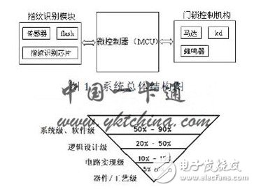
The entire door lock system is powered by 4 AA batteries. Therefore, power consumption is one of the important factors affecting the success or failure of the system. A complete low-power design can run through the entire digital system design process from system design, software design, logic design, circuit implementation to the device/process level. The low-power effects that can be achieved at each level are different. The higher the abstraction level, the greater the space for optimization and the more obvious the effect. Figure 2 shows the system power consumption that can be reduced by different levels of low-power design [1].
The system design layer determines the performance requirements of the system and divides the software and hardware. The power consumption optimization made at this layer is mainly based on the system function description for software and hardware co-design to obtain the best performance/power ratio. The software design layer generates the code that is finally executed on the system hardware. The power consumption optimization made at this level is mainly to make full use of the power saving mode provided by the hardware, and to rationalize the working status of each device; the logic design layer determines the application system The hardware structure to be used in the production of components. For the microcontroller, the power consumption optimization at this stage mainly considers the optimized design of the system clock and processor instructions. Reasonably arrange the communication of each module in the system; the circuit implementation layer mainly considers power consumption optimization from the perspective of reasonable layout and routing on the chip; the device process layer mainly considers power consumption optimization from the chip manufacturing process and materials. This article mainly reduces system power consumption from the following aspects:
1) Device selection: According to the hardware determined by the system design layer, try to choose hardware with low power consumption. The method starts with the hardware with high power consumption. For example, the MCU of this system uses Mega88, which is a monolithic package. MCU is suitable for many occasions requiring high integration, low cost, and low power consumption, and can meet various performance requirements.
2) System working mode selection: try to choose high-speed and low-frequency working mode as much as possible. Almost all CMOS devices are used in low-power systems, because their level changes quickly, which is beneficial to reduce power consumption; in addition, the input terminals that are not used by CMOS circuits have protection circuits , But it can’t be left floating, lest the input logic level is uncertain, the circuit flips back and forth, and the system power consumption is increased. In this paper, the idle pins of Mega88 are all used to output high level, and the internal 1M clock frequency is used. Make full use of the "idle" and "power-down" modes. In this article, Mega88 uses the power-down mode when the system is idle. In this mode, the MCU's quiescent current is only 5 microamperes.
3) Reasonable power management: The fingerprint lock system is idle most of the time. According to this fact, it only enters the working state when the system is working, and the MCU is in the power-down state at other times. In addition, not all peripherals of the system need to work during the working period. If the system keeps supplying power to these devices during the working period, it will cause a huge waste of energy. In this case, the circuit can be designed as a module, and the module can be supplied with intermittent power supply during operation, so that the module circuit is only powered on for a short period of time when it needs to work, and the rest are in a power-off state.
4 Fingerprint recognition module designThe fingerprint recognition module is composed of a fingerprint recognition chip, a fingerprint sensor, and a flash memory that stores fingerprint template information. The fingerprint recognition chip is the core module in the fingerprint recognition module and is responsible for fingerprint image processing. It is connected to Mega88 via UART, as shown in Figure 2. Show.
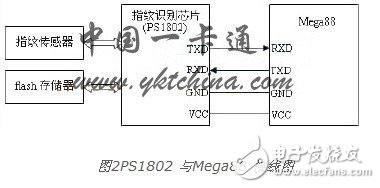
Mega88 uses the UART port to control the fingerprint recognition chip to perform a series of image processing operations such as fingerprint image acquisition, feature extraction, fingerprint feature comparison, and generation of fingerprint feature templates according to the communication protocol in the PS1802 programming manual, and save the generated feature templates. In the flash, the specific implementation method can refer to the PS1802 programming manual [3]. In order to reduce the power consumption of the system, the power supply of PS1802 is controlled by an electronic switch. The power supply is turned on only when fingerprint operation is performed. It takes a while for PS1802 to reset. Therefore, when PS1802 is powered on, the image acquisition command cannot be sent immediately. It should be delayed. For a period of time, based on empirical values, 200ms is the best.
5 Infrared interface module designFigure 3 is a schematic diagram of IRM5000D work. Among them, IRM5000D is an infrared data transponder. When sending data, the receiving pin (RxD) is quiet, thereby improving the accuracy of communication; it supports power-down mode, by setting the SD pin high Level, the quiescent current of IRM5000D is less than 0.01 microampere.
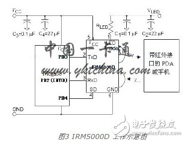
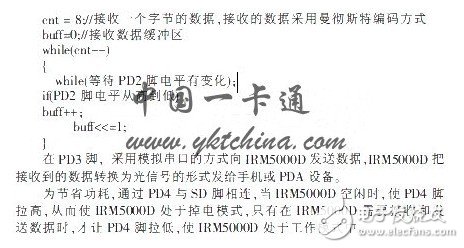
As shown in Figure 3, Mega88 is connected to the receiver (RxD) and transmitter (TxD) of the IRM5000D through PD2 and PD3, respectively. In order to receive the infrared signal sent by the PDA in real time, Mega88 receives data by starting the external interrupt 0 and monitoring the PD2 pin level change in the interrupt handler. The external interrupt 0 adopts the low-level trigger mode. In order to achieve the wake-up interrupt mode, press With a baud rate of 9600bit/s, each data sent by the PDA must be preceded by a byte of wake-up header (0x00), and its communication format is: "0x00+data". In order to receive data according to level changes, data Some use Manchester encoding. The following is the implementation code in the interrupt handler:
This article introduces a design scheme of a low-power fingerprint lock with infrared interface, focusing on a low-power design method. According to this method, the quiescent current of the fingerprint lock designed in this article is only 15 microamperes, which can fully meet the requirements of industrial products. Design requirements. In addition, the most important fingerprint module and infrared interface module in the system are also introduced in more detail.
Solar home energy storage power supply
SHENZHEN CHONDEKUAI TECHNOLOGY CO.LTD , https://www.szfourinone.com