Circuit board design and implementation of electronic design competition with FPGA as the core control
Undergraduate electronic competition topics are based on analog electronics, digital electronics, programmable logic devices and single-chip technology, and involve multi-disciplinary content such as electronic instrumentation, communications, high-frequency radio, and automatic control. The 2007 electronic design competition organizing committee experts pointed out: The development trend of electronic design competition will focus on analog, digital, and FP2GA. Therefore, it is very important for the team members to choose suitable topics and conduct training to obtain better results. The author designed and produced the competition circuit board in accordance with the characteristics of the competition topic and the requirements of competition components with FPGA as the core. The composition block diagram is shown in Figure 1.
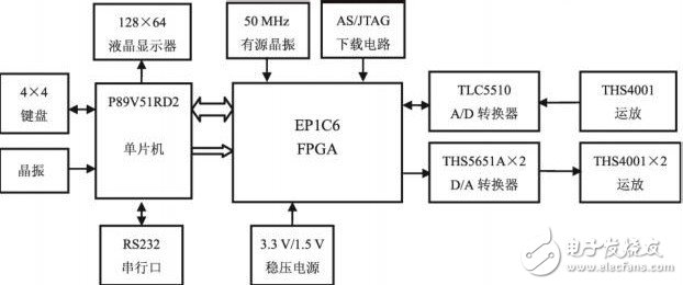
Figure 1 Block diagram of electronic competition circuit board
This design mainly includes 3 parts: MCU expansion circuit, FPGA core circuit, high-speed A/D and D/A conversion circuit. The extended circuit of the single-chip microcomputer mainly includes the oscillation circuit, the interface of the liquid crystal display module, the button, the reset circuit, etc. This part can not only perform basic single-chip experiments, but also provide control signals for the FPGA core circuit and use FPGA resources; FPGA core circuit part Mainly composed of power supply, J TAG download, AS download, input and output circuit, etc.; high-speed A/D and D/A conversion circuit has one analog signal input and two analog signal outputs. The design organically combines the three parts to form an experimental system, which can not only complete the design of competition topics such as equal-precision frequency meters, DDS signal generators, and digital oscilloscopes, but also be used for pre-match training.
1 Circuit design 1. 1 FPGA core circuit board. 1. 1. 1 FPGA chip selectionFPGA is the abbreviation of English Field Programmable Gate Array, that is, field programmable gate array. It is a product of further development on the basis of PAL, GAL, EPLD and other programmable devices. It emerged as a semi-custom circuit in the field of application-specific integrated circuits (ASIC), which not only solves the shortcomings of custom circuits, but also overcomes the shortcomings of the limited number of gate circuits of the original programmable devices.
After analyzing the topics in recent electronic design competitions, it is found that the design topics do not have too high functional requirements for FPGAs. Generally, commonly used FPGAs can meet the design requirements. Through comparison, we know that Altera's Cyclone series FPGAs have low-cost features, and they balance logic, memory, phase-locked loops, and advanced I/O interfaces. So Cyclone series FPGA is the best choice for design.
The EP1C3, EP1C6, and EP1C12 in Altera's Cyclone series can fully meet the requirements of the design problem, so you can choose FPGA from these types of chips. The EP1C6 series of chips are selected for comprehensive comparison. The EP1C6T 144C8 in this series can fully meet the requirements of the electronic competition. Claim. And EP1C6T 144C8 also supports SOPC (System On Pr ogrammingChip), which can realize embedded soft CPU (such as NIOSII, etc.), providing another option for embedded electronic design. So here we choose EP1C6T144C8 as the FPGA chip of this design. EP1C6T144C8 has 5,980 logic units (LE), 20 M4K RAM blocks, 92 160-bit embedded RAM, 2 phase-locked loops, 96 I/O ports, supports AS and JTAG downloads, and adopts TQFP144 packaging.
1. 1. 2 FPGA circuit board designEP1C6T144C8 is a 144-pin FPGA chip. The pin classification and functions are as follows:
(1) Power supply pin. Using a voltage of 3.3 V as a power supply can provide power for output buffers that meet various data transmission standards, and can also provide power for input buffers that meet LVT TL, LVCMOS, and various PCI interface standards.
(2) The power supply pin of the internal logic gate. Using 11 5 V voltage as the power supply, it can provide power for the input buffers that meet the LVDS, SSTL2, and SST L3 interface standards.
(3) The power supply pin of the phase-locked loop. Regardless of whether the PLL power supply is used or not, this pin must be connected to the 11 5 V power supply.
(4) Configure the pins. Including the JTAG boundary scan test configuration interface and AS active serial configuration interface.
(5) User I/O port pins. There are 96 user I/O pins of the FPGA chip, which are led out through double-row sockets. These interfaces are divided into 3 categories: interface with single-chip microcomputer, expansion interface, interface with A/D converter and D/A converter.
(6) Clock pin. Using 50 MH z active crystal oscillator, the output clock signal is buffered by a low-resistance resistor and then connected to CLK0, which is the pin 16 of the FPGA.
1. 2 MCU expansion interface circuit design 1. 2. 1 MCUAs the de facto industry standard for 8-bit microcontrollers, the 80C51 series of single-chip microcomputers are produced by many electrical companies in the world, with a wide range of choices and application foundations. Such as AT 89C5X, AT89S5X of ATMEL Company, P89C5X, P89V5X of NXP Company and so on. In this design, the P89V51RD2 microcontroller of NXP Company was selected. The microcontroller has 64 K bytes of repeatedly erasable and online downloadable programming (ISP) FLASH program memory, 256 bytes of RAM, and 1 K bytes of extended RAM. , 32 I/O ports, 3 programmable timer counters, a serial port, an SPI interface and other functions.
1. 2. 2 LCD moduleUsing 128@64 graphic dot matrix LCD display module with Chinese Chinese character library, containing 8 192 16@16 dot Chinese characters and 128 16@8 half-width letter symbol fonts; in addition, the graphic display screen provides a 64@ 256-dot drawing area GDRAM; and contains CGRAM to provide 4 groups of software programmable 16@16 dot matrix character creation functions. The power supply has a wide operating range (21 7 V to 51 5 V), and the low-power design can meet the power-saving requirements of the product; at the same time, the interface with the microcontroller and other microcontrollers is flexible (3 modes: parallel 8-bit/4-bit, serial Line 3 lines/2 lines).
The Chinese liquid crystal display module can realize the same screen display of Chinese characters, ASCII codes, and dot matrix graphics. It is widely used in various instruments, household appliances and information products, and as a display device. The Chinese liquid crystal display module has commands to move the current display screen up/down/left/right and clear the screen, cursor display/flicker control commands and close display commands. A variety of control lines (reset/serial and parallel selection/brightness adjustment) are reserved for users to use flexibly.
1. 2. 3 KeyboardExpand 16 buttons to form a 4@4 matrix and connect to the P1 port of the single-chip microcomputer.
1. 2. 4 Interface with FPGAThe P0 port, P2 port, RD, WR, and ALE of the single-chip microcomputer are respectively connected to the FPGA reserved I/O ports through 100 8 resistors.
1. 2. 5 RS232 interfaceExpanding the MAX232 serial port chip and expanding the serial port can realize the serial communication between the single-chip computer and the PC, and online downloading of programs.
1. 3 High-speed analog-to-digital converter and digital-to-analog converter circuit 1. 3. 1 High-speed analog-to-digital converterBecause FPGA is a high-speed device, in order to achieve speed matching, this design uses a high-speed A/D converter TLC5510. It is a new type of analog-to-digital conversion device (ADC) produced by the American TI company. It is an 8-bit high-speed device manufactured by CMOS technology. Impedance parallel A/D conversion chip, the highest sampling rate that can be provided is 20MSPS. Because TLC5510 adopts half-flash structure and CMOS process, it greatly reduces the number of comparators in the device, and can keep low while converting at high speed Power consumption. Under the recommended working conditions, the power consumption of the TLC5510 is only 130 mW. Because the TLC5510 not only has a high-speed A/D conversion function, but also has an internal sample-and-hold circuit, which greatly simplifies the design of the peripheral circuit. At the same time, because of its internal standard voltage divider resistors, a 2 V full-scale reference voltage can be obtained from a +5 V power supply. TLC5510 can be applied to digital TV, medical imaging, video conferencing, high-speed data conversion, and QAM demodulators. T LC5510 is a 24-pin, SO, PSOP surface-mount package.
1. 3. 2 High-speed digital-to-analog converterThe high-speed D/A converter uses the TH S5651A produced by TI. This chip is a 10-bit digital-to-analog converter specially optimized for wired and wireless data transmission. The chip is manufactured using advanced high-speed mixed-signal CMOS technology, with a conversion rate of 125 MSPS. On-chip has a 11 2 V reference voltage, D/A conversion output is current type, and the current range is 2 mA-20 mA. The power consumption is 5 V is 175 mW when working, 25 mW when working in SLEEP mode, and the package is 282-pin SOIC or TSSOP package.
1. 3. 3 High-speed operational amplifierIn order to match the speed of the high-speed A/D and D/A converters, the TH S4001 high-speed voltage negative feedback operational amplifier produced by the American TI company is also used in the circuit design. With a bandwidth of up to 270 MHz and a conversion rate of up to 400 V/Ls, it can well realize the system's amplification and buffering function to meet system performance requirements.
2 ConclusionThe electronic competition circuit board of this design adopts MCU + FPGA structure, the single-chip computer is responsible for data processing, control and display, etc.; FPGA is responsible for high-speed data acquisition and digital-to-analog conversion. At the same time, FPGA can also provide resources such as memory and I/O ports for the microcontroller. In PCB design, special attention should be paid to anti-interference measures, such as proper configuration of decoupling capacitors in the circuit, separation of digital ground and analog ground, and finally connection to the power ground at one point. This design uses shielded ground, digital ground and analog ground in the design of the ground wire, which are connected to the power ground respectively, so that the digital current does not flow through the analog device, and the high-speed current does not flow through the low-speed device. Through debugging, the circuit involved in this article can achieve the expected function of each module. The circuit board can be used in electronic design competitions and the development of some electronic products.
This is a special maskking High GTS e-cigarette product series. We sell maskking high gts vape, mk HIGH GT Vape, and maskking high gts flavors.
We are specialized electronic cigarette manufacturers from China, Vapes For Smoking, Vape Pen Kits suppliers/factory, wholesale high-quality
products of Modern E-Cigarette R & D and manufacturing, we have the perfect after-sales service and technical support. Look forward to
your cooperation!
maskking high gts vape pen, maskking high gt vape 2500 puffs,maskking high gts vape kit,mk high gts vape,maskking high gts e-cigarette
Ningbo Autrends International Trade Co.,Ltd. , https://www.mosvape.com