Design of digital video monitoring unit
Abstract: This paper introduces a video surveillance system based on embedded platform. Using TMS320DM365 as the core processor, an intelligent digital video monitoring unit is designed in a modular way. The unit includes video capture input, external memory, Ethernet and video output. The design utilizes the multi-peripheral interface feature of the TMS320DM365 and uses four chips to meet its video processing capabilities. The video capture input of the unit uses TVP5158 video decoder, DDR2 SDRAM uses W971GG6IB, NAND FLASH is K9F2808U0C, and Ethernet controller adopts ENC28J60. The system's processor core operates at speeds up to 300 MHz.
Keywords: TMS320DM365; digital video; monitoring; peripheral interface
This article refers to the address: http://
0 Introduction Video surveillance systems have been widely used in daily life, and their stable and reliable work has become a necessary condition to ensure the normal operation of people's production and life. Reliable and fast acquisition of input, codec, and processing transmissions is a key point in the design of video processing equipment. This article describes a digital video unit based on DaVinci technology. The unit mainly completes the intelligent collection and processing function of the video information and the integrated image processing function.
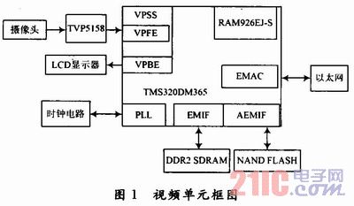
1 Video unit composition and hardware design The video unit uses TMS320DM365 as the core processor chip, and designs video buffering and video decoding functions based on TMS320DM365. The hardware of the unit mainly includes DaVinci processor chip (TMS320DM365, hereinafter referred to as DM365), video decoder chip (TVP5158), DDR2 SDRAM, FLASH, ENC28J60 Ethernet controller, power management chip and so on. The block diagram of the video unit is shown in Figure 1. This article mainly introduces the video capture input part, the external memory part, the Ethernet part and the video output part.
The DM365 is highly integrated with a wide range of components, including H. 264, MPEG-4, MPEG-2, MJPEG and VC1 codecs, integrated image signal processing (ISP) solutions for intelligent video processing functions and a range of onboard peripherals, reducing system cost.
The working principle of the video unit is as follows: The TVP5158 video decoding chip performs analog-to-digital conversion on the analog video signal transmitted from the CCD camera to become conforming to ITU-R BT. 656 or YUV standard digital video signal; then the digital video signal is transmitted to the front end of the video processing subsystem of the Finch processor, preprocessed and sent to the back end of the video processing subsystem, the back end of the video processing subsystem The digital video signal is encoded and output directly to the display terminal. The ARM terminal on the DM365 is mainly used as a controller to control the video decoding chip and the peripheral interface chip.
1.1 Video Capture Input Design The camera transmits the acquired analog video signal to the TVP5158 video decoder. The TVP5158 device is a 4-channel, high quality NTSC/PAL video decoder that digitally encodes all baseband analog video formats into digital video signal outputs. Each channel of the encoder contains a 10-bit 27 MSPS analog-to-digital converter. The TVP5158 supports NTSC (J, M, 4.43) and PAL (B, D, G, H, I, M, N, Nc, 60) standard video simultaneous input. Composite video input is supported for each video decode channel. The TVP5158 output port supports 8-bit ITU-R BT, 656 and 16-bit 4:2:2 YUV formats. The TVP5158 video decoder then transmits the decoded signal to the DM365's Video Processing Front End (VPFE). The TVP5158's highly flexible video output seamless interface to the DM3 65 eliminates the need for an external FPGA. The interface block diagram of TVP5158 and DM365 is shown as in Fig. 2.
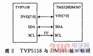
TVP5158 outputs 8-bit ITU-RBT. 656 and 16 bit 4:2:2 YUV format video. DM365 supports ITU-BT. 601/BT. 656/BT. 1120 digital YCbCr 4:2:2 (8 b/16 b) format video, so DM365 in this system uses YCbCr 4:2:2 8-bit ITU-R BT. 656 video capture mode, the system does not require an external line/field sync signal. The DVO pin of the TVP5158 is connected to the YIN pin of the DM365 for data transfer.
1.2 External Memory Design In this unit, the external memory selected is a DDR2 SDRAM chip and a NAND FLASH chip. In this unit, Winbond Electronics' 1 GB DDR2 SDRAM is used as the main memory, model number W971GG6IB. The interface block diagram of DM365 and W971GG6IB is shown in Figure 3.
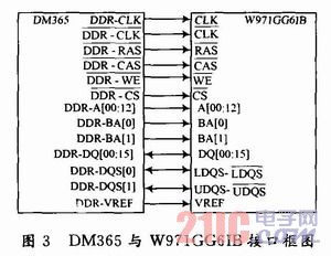
CLK and the clock signal pin, the chip clock is input through these two pins. The row address is latched, the column address is latched, and the write enable is enabled. These three pins specify the input command. When the chip is selected high, all external commands are disabled; external group selection is also available. A0 ~ A12 is the address bus, the row address in the chip is A0 ~ A12, the column address is A0 ~ A9, and A10 is the automatic pre-charge flag. Because the unit uses a 1 GB DDR2 SDRAM, the BA0 and BA1 pins are selected to select the eight groups in the chip. DQ0~DQ15 are bidirectional data bus pins that support 16-bit wide data transmission. When the DDR-DQS is written, the data is output to the chip; when the DDR-DQS is read, the data of the chip is input to the DM365. DDR-DQS1 is used for DDR-DQ[15:8] and DDR-DQS0 is used for DDR-DQ[7:0]. LDQS is connected to DDR-DQS0, LDQS corresponds to data on DQ0 to DQ7; UDQS is connected to DDR-DQS1, and UDQS corresponds to data on DQ8 to DQ15. LDQS and UDQS are low and high data strobes, respectively, and are only used when different data strobe modes are enabled by the EMR control bits.
The NAND FLASH selected in the unit is Samsung's K9F2808UOC, which is a 132 MB flash memory with a memory capacity of 16M×8 b capacity and 4 MB spare capacity. The memory array contains 1,024 individually erasable blocks, each of which contains 16KB. The eight I/O pins of the K9F2808U0C are address multiplexed, which reduces pin count and facilitates system upgrades. The flash power supply is 3.3 V. The interface block diagram of DM365 and K9F2808U0C is shown in Figure 4.
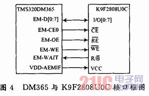
In Figure 4, I/O0~I/O7 are data input/output pins connected to the EM-D[O:7] pin for data transmission. I/O pins are used to input commands, addresses, and data, and are also used to output data during a read operation. The pin is connected to the EM-CE0 pin for chip select function. The pin is connected to the EM-OE pin to control the serial data output. The pin is connected to the EM-WE pin and controls the writing to the I/O port. Commands, addresses, and data are locked on the rising edge of the pulse. The output pin, connected to the EM-WAIT pin, indicates the state of the device operation. When low, it indicates that a program, erase or random read operation is in progress, and returns to high level after the end. status.
1.3 Ethernet Design The DM365 communicates with the network through the ENC28J60 Ethernet controller. The interface block diagram is shown in Figure 5.
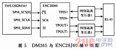
The ENC28J60 Ethernet Controller is a product from Microchip Technology Inc. for thin embedded network applications. The SPI interface of the DM365 is connected to the SPI interface of the ENC28J60 chip. For the chip select input pin, SCK is the clock input pin and SI is the data input pin. Two network transformers need to be connected between the ENC28J60 chip and the RJ-45 interface. Connect a 1:1 pulse transformer dedicated to 10BASE-T operation on the differential receive pin (TPIN+/TPIN-); connect a 1:1 pulse with center tap on the differential transmit pin (TPOUT+/TPOUT-) transformer. The transformer acts as a level shifter and electrical isolation.
1.4 Video Output Design The LCD display is connected to the video processing back end. The block diagram of the video output section is shown in Figure 6.
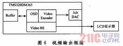
The main function of the OSD module is to capture and mix video data as well as display/bitmap data and transmit them to the Video Encoder (VENC) in YCbCr format. Video and display data are read from external DDR2/mDDR memory.
2 Conclusion This design uses DM365 video processing chip, making full use of its peripheral interface features, select some peripheral interface chips to meet the intelligent video processing functions.
Substation Transformer,Prefabricated Substation,High Quality Prefabricated Substation,European Type Substation
Hangzhou Qiantang River Electric Group Co., Ltd.(QRE) , https://www.qretransformer.com