Those pits in the op amp - the first
1. One of the ten pits of the operational amplifier - rail-to-rail
After the output voltage of the op amp could not reach the power rail, I chose the rail-to-rail op amp, haha, so that the op amp can finally be output to the power rail. Behind the happy is a hidden big pit waiting for me:
Take a look at a company I'm using for rail-to-rail op amp products: "High-speed (>50MHz) rail-to-rail op amps support lower supply voltages, closer power rail swings, and wider dynamic range ."Do you see it:
“Works with a lower supply voltage, closer to the rail of the supply rail, and a wider dynamic range.â€
"Closer to the swing of the power rail"
"Closer"
"close"
. . .
Look at the manual for a rail-to-rail op amp:

The output voltage is really not 5V of the power supply, why?
The output stage of an op amp can be simplified to the following form of structure:
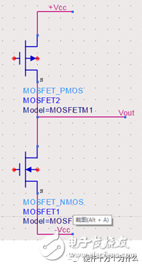
Since the MOS transistor has an on-resistance, when a current flows, a voltage drop is caused. Therefore, when the load is larger, the on-state voltage drop is larger, and the output voltage is less likely to reach the rail.
Therefore, the rail-to-rail op amp is not completely able to make the output reach the power supply value. When it is used, it is necessary to look at the relationship between the load and the temperature (affecting the resistance of the on-resistance) to determine how much the output can reach.
2, the second step of the op amp - non-negligible input bias current
A voltage divider circuit is designed. In theory, input 1V, output 2V, but one test, always more than 6,7 mV. This is to enter the 12-bit 3V range ADC, but to eat more than 600 yards.
The positive input and reverse inputs of the op amp resulted in input bias currents at the two inputs due to TVS leakage current and tube input bias current (and because no one device is identical to the other, both The input bias currents are not the same); these two bias currents form a bias voltage with the external resistor and output to the back end, creating an error . If you accidentally choose a BJT-based op amp that has a large input bias current, it will cause a large back-end error. As shown in the figure below, this kind of op amp is really "stopping at the big, it is simply awkward."

The following assumes that the input bias currents of the two inputs are the same.
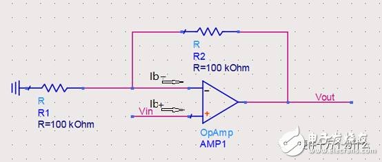
For the forward input, Ib+ brings the bias voltage to be almost equal to 0, and for the inverting input, Ib- brings the bias voltage equal to 350mV (when calculating, assume Vout is grounded, equivalent to R1/ /R2). Therefore, what is needed is to add a resistor to the forward input to compensate for the error caused by the inverting input.
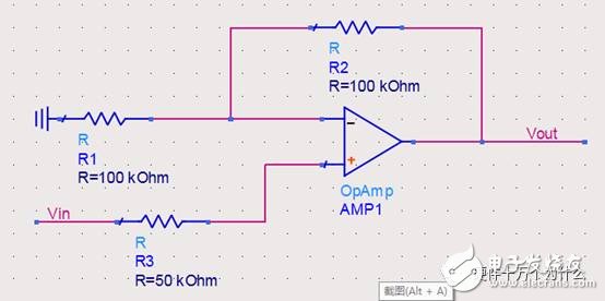
As mentioned earlier, the positive and negative input bias currents are not the same, the compensation can only reduce the offset voltage, and the positive and negative input bias current difference is also called the offset current . When performing high-precision or small-signal sampling, a low-offset current op amp can be selected. Because the compensation resistor is added, a new noise source is also added, which should be carefully added.
The bias current is one of the main errors of the op amp. In the following pits, some error sources that affect the post-stage are also introduced.
3, the third of the three holes of the operational amplifier - the rapid decline of PSRR
When I was a rookie engineer, the op amp design never considered PSRR. When I heard about PSRR, each op amp would choose an op amp with a higher PSRR based on cost control.
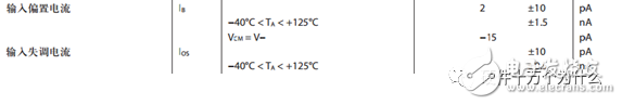
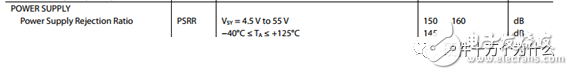
For example, this op amp PSRR has reached 160dB:
According to the calculation formula:

Even if the supply voltage changes between 4.5V and 5.5V, the effect of the power supply on the output of the op amp is only 10nV.
Unfortunately, this indicator refers to the DC change of the power supply voltage, and does not include changes in the power supply voltage exchange (such as ripple). In the case of AC, this indicator will be greatly deteriorated. What is mentioned in Spec. is only the DC change. The change of communication is shown in the figure below. Under normal circumstances, the non-senior engineers treat the illustrations smoothly and slid over.
If the op amp circuit uses a switching power supply and does not perform decoupling and filtering well, the input accuracy of the latter stage will be greatly affected. Look at the exchange PSRR of the same op amp.
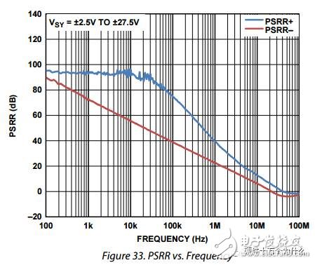
For the 500kHz switching frequency ripple, PSRR+ deteriorates to only 50dB. Assuming a ripple size of 100mV, the effect on the post-stage will deteriorate to 0.3mV. For many small signal acquisition applications, this error is unacceptable. Therefore, some applications even make a low-pass filter at the op amp power inlet (note the resistor power and resistor thermal noise ).
4, the fourth of the ten-hole of the operational amplifier - the chaotic compensation capacitor
In the past, an "old engineer" told me that the feedback circuit adds a capacitor and the circuit will not oscillate. As soon as I saw the words "shock" so high, I was forced on the spot. All the circuits in the future were combined with a small capacitor, so that they were professional.
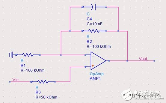
Until one day, I want to amplify a signal of 100kHz (good luck, frequency is not too high, otherwise the voltage feedback op amp can not play), also according to experience and a capacitor, and then. . . The signal is no longer normal. . . Because, this capacitive feedback impedance is reduced to less than 200Ω for a 100kHz signal, resulting in a change in the amplification factor.
Of course, this is not the key. The question is: Do you really need a compensation capacitor?
Â
First, there is a pole inside the op amp (it thinks it is caused by RC low-pass), which causes a phase change, up to -90°:
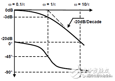
If you add another pole, it will change the phase again, and the maximum can be increased to 90°:
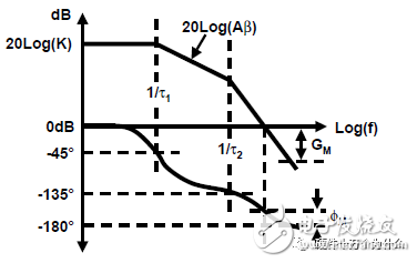
So the phase is -180°, what's the problem? That is the "shock." Take a look at the gain of the voltage negative feedback op amp:
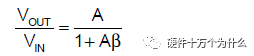
When the loop gain Aβ at some frequency points is equal to 1 and the phase is -180°, then Vout/Vin will become infinite and the circuit will be unstable. Therefore, when a zero is added externally, the op amp will enter the oscillation at some frequency points , such as the distributed capacitance on the pin, as shown below:
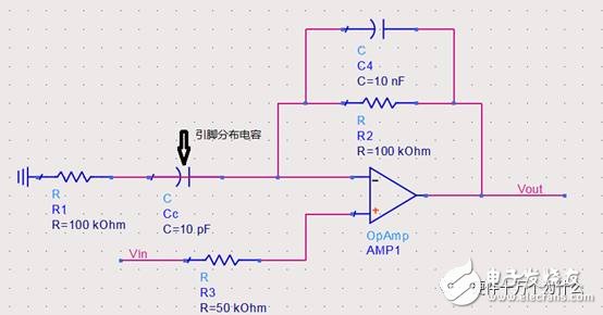
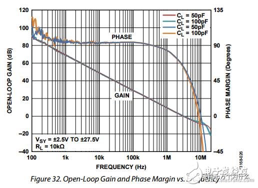
At this time, we put on a capacitor, which is equivalent to artificially introducing a zero point and pulling the pulled down phase . However, this distributed capacitance is generally small, so that its loop gain Aβ is equal to 1 and the position is very far. At the frequency, the op amp has not been working properly. Looking at the manual, the op amp itself is at 100k, the phase margin is quite high, exceeding 90°, and there is no need to add additional compensation capacitors.
Therefore, for the specific situation, we must analyze it in detail and cannot be carried away by the "old engineer".
5, the fifth of the ten-hole of the operational amplifier - the common mode input range of the bedding
I have encountered a problem before, the preamplifier is amplified, and then the op amp follows the ADC, the signal into the ADC is 0.3V-1.5V. It feels like a very simple circuit, but the actual measured voltage is a single-power 5V op amp. When some boards are outputting about 1.5V, its output value does not completely follow the input value, but lower than the ratio. The 1.5V signal is no problem to follow, but it is not right once it is close.
Of course, this question went to the meeting of the hardware group. The final result of the discussion was: "There is a problem with this op amp. We are looking for manufacturers to sell the discs, but we are xx companies, and we don't care about us, so let's change. An op amp from another company." Unfortunately, we picked up an op amp and didn't find the cause of the problem. Fortunately, we didn't fully understand the principle, we happened to choose a working op amp.
Looking at an indicator of this op amp, the op amp's common-mode input range:
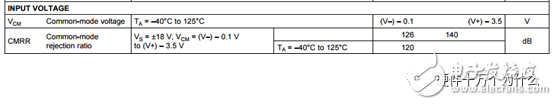
The op amp's common-mode input range is an interval of the op amp's input voltage. It characterizes the interval in which the op amp can operate linearly. That is, the input voltage common-mode value is within this interval. When the input voltage changes, the output voltage can be linear. A change has occurred.
For the follower circuit, due to the negative feedback, the positive phase input terminal voltage and the negative phase input terminal voltage are basically the same value, and the common mode input range is -0.1V to the 5V power supply. 1.5V. Therefore, when the input voltage is around 1.5V, there is a case where the op amp cannot be linearly followed normally.
Why can't you follow? Let's look at a triode amplifier circuit, which is also part of the op amp, for illustration.
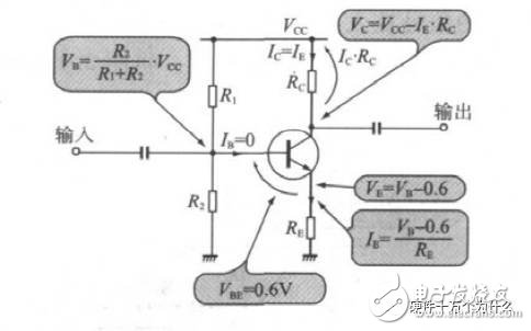
When the input Vb changes, Ie will change correspondingly with Vb, causing Vc to change, which is followed. If Vb continues to increase to Vc=Vcc-Ie x Rc, the calculated value is negative, but in fact Ie x Rc cannot exceed Vcc. At this time, the amplifying circuit reaches saturation or even the current is inverted, resulting in fixed or cut output voltage. Peak or reverse, etc.

Silicone Rubber keypads (also known as elastomeric keypads) are used extensively in both consumer and industrial electronic products as a low cost and reliable switching solution.
Silicone Rubber Keypads,Membrane Keyboard Switch,Silicone Rubber Waterproof Keypads,Silicone Rubber Numeric Keypad
KEDA MEMBRANE TECHNOLOGY CO., LTD , https://www.kedamembrane.com