High-power lighting class LED packaging technology, material details
From a practical point of view, high-power LED devices that are simple to install and relatively small in size will replace traditional low-power LED devices in most lighting applications. In order to meet the needs of lighting, lighting fixtures composed of low-power LEDs must concentrate the light energy of many LEDs to meet the design requirements, but the disadvantages are that the wiring is extremely complicated and the heat dissipation is not smooth. In order to balance the current between the LEDs, For voltage relationships, complex power supply circuits must be designed.
In contrast, the power of the high-power single-chip LED is much larger than the sum of the power of several small-power LEDs, the power supply line is relatively simple, the heat dissipation structure is perfect, and the physical characteristics are stable. Therefore, the packaging method and packaging material of the high-power LED device cannot simply apply the packaging method and packaging material of the conventional low-power LED device. Large dissipated power, large heat generation and high light extraction efficiency put new and higher requirements on LED packaging technology , packaging equipment and packaging materials.
1, high power LED chip
In order to get a high-power LED device, it is necessary to prepare a suitable high-power LED chip. The international methods for manufacturing high-power LED chips are as follows:
1 increase the size method. By increasing the effective light-emitting area and size of the individual LEDs, the current flowing through the TCL layer is evenly distributed to achieve the desired luminous flux. However, simply increasing the light-emitting area does not solve the heat dissipation problem and the light-emitting problem, and does not achieve the expected luminous flux and practical application effects.
2 silicon floor flip method. Firstly, a large-sized LED chip suitable for eutectic soldering is prepared, and a silicon substrate of a corresponding size is prepared, and a gold conductive layer for eutectic soldering and a conductive layer (ultrasonic gold ball solder joint) are formed on the silicon substrate. Then, the eutectic soldering device is used to solder the large-sized LED chip to the silicon substrate. This kind of structure is more reasonable, considering both the light-emitting problem and the heat-dissipation problem, which is the current mainstream high-power LED production method.
LumiLEDs developed the AlGaInN power flip-chip (FCLED) structure in 2001. The manufacturing process is: firstly deposit a NiAu layer with a thickness greater than 500A on the P-type GaN on top of the epitaxial wafer for ohmic contact and back. Reflection; then using a mask to selectively etch away the P-type layer and the multi-quantum well active layer, exposing the N-type layer; forming and etching to form an N-type ohmic contact layer, the chip size is 1 mm × 1 mm, P-type ohmic contact In a square shape, an N-type ohmic contact is inserted in a comb shape, which shortens the current spreading distance and minimizes the expansion resistance; then, the metal bumped AlGaInN chip is flip-chip bonded to the silicon with an antistatic protection diode (ESD) On the carrier.
3 ceramic floor flip method. Firstly, an LED chip with a large light-emitting area suitable for the eutectic soldering electrode structure and a corresponding ceramic substrate are prepared by using an LED chip general-purpose device, and a eutectic soldering conductive layer and a conductive layer are formed on the ceramic substrate, and then eutectic soldering is performed. The device solders large LED chips to the ceramic backplane. Such a structure not only considers the light-emitting problem but also the heat-dissipation problem, and the ceramic bottom plate is a high-heat-conducting ceramic plate, the heat dissipation effect is very ideal, and the price is relatively low, so it is a suitable floor material at present, and can be used for the future. Integrated circuit integrated package reserved space.
Medical Aid Equipment Wire Harness
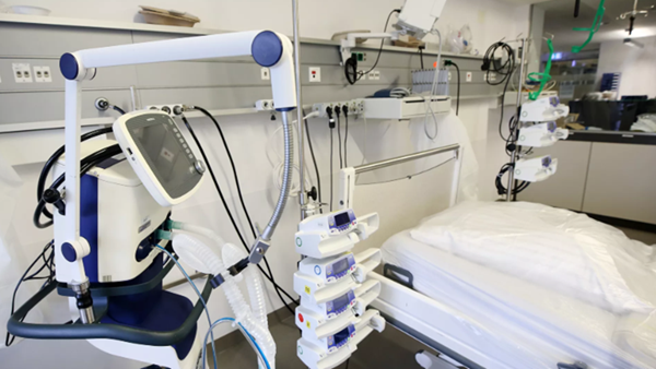
The wiring harness for medical rescue equipment refers to the wiring harness applied to various medical rescue equipment. Emergency medical equipment, that is, the medical equipment used in emergency treatment, refers to the emergency medical equipment used by the rescuer when any accident or emergency occurs.
Before arrival, in accordance with the principles of medical care, use on-site applicable medical equipment to temporarily and appropriately perform preliminary rescue and care for the wounded and sick.
Kable-X provides various connecting harness components for medical device maple equipment. These wiring harness not only meet the needs of signal transmission and high-voltage contacts, electrical appliances and machinery, but also provide reliable and stable quality for customers' special application requirements, most of which are used for Computer tomography equipment, movable auxiliary equipment, solutions for increasing demand, medical electronic beds, rotatable chairs and wheelchair controllers.
We produce a large number of Medical Cable Assembly, including Ventilator Wire Harness, Medical Defibrillator Wire Harness and Medical Aid Equipment Wire Harness .

Medical Aid Equipment Wire Harness,Medical Equipment Wire Harness,Medical Custom Cable Harness,Medical Aid Equipment Wire Harness For Sale
Kable-X Technology (Suzhou) Co., Ltd , https://www.kable-x-tech.com