How to DIY a long life and expandable flash memory smart lock
As more and more building and residential owners want to transform the smart locks or electronic locks of their buildings and residences, this makes battery-powered wireless smart locks more and more popular in today's market.
In smart lock applications, high-current motors and radios usually consume more power, which affects battery life. Replacing multiple batteries can be time-consuming and costly, so reducing average current consumption is usually a key design consideration.

This design is supported by TI’s light-load high-efficiency DC/DC converter, SimpleLink™ ultra-low-power wireless MCU platform, integrated motor driver and RGB LED driver. This design covers a wide range and helps system designers in electronic locks, Access control keyboards and readers, wireless automatic blinds, and HVAC dampers and actuators in the design of low-power door locks take the lead.
1. System principle
The design uses a CC2640R2F MCU with integrated Bluetooth Low Energy (BLE) radio to wirelessly lock and unlock the door. At the same time, it can monitor the battery voltage to indicate the end of life state and limit the current flowing through the motor (helping to extend the life of the motor ) And use LED lighting and graphics to convey related events to users.
The design achieves extremely long battery life by selecting the power supply topology (in this case, the high-efficiency buck converter TPS62745) and extending the duty cycle of Bluetooth low energy connection events.
Various smart lock systems usually contain four main components: MCU, low-power Bluetooth radio, motor driver and power management.
After calculating the average power consumption of each device, the battery life (in milliwatt hours) can be calculated. To calculate battery life, two different current schemes need to be studied:
â‘ Bluetooth is turned on and a connection event is sent every 500ms (or any other value selected by the user).
â‘¡ The lock or unlock event sends a signal to the motor driver, instructing the driver to provide about 1A current through the DC motor.
We will ignore the Bluetooth pairing time, because it usually means that an event is about to happen, and the current provided by the motor is almost two orders of magnitude higher than the current flowing into the Bluetooth device.
The events mentioned in this design refer to locked or unlocked situations. For example, if a user unlocks a door and then locks it again, this is considered as two events (one is a lock event and the other is an unlock event).
This design considers two main factors when choosing a battery: capacity and the popularity of the battery platform. The capacity of AA batteries is greater than that of AAA batteries.
In addition, more applications similar to smart dampers on the market today choose to use AA batteries.
2. System block diagram
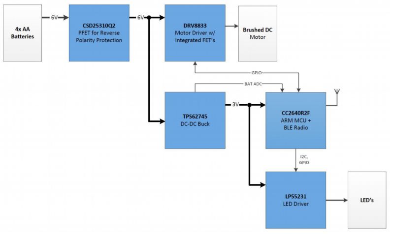
3. Core device
DRV8833: Dual H-bridge motor driver with motor current control function and 360mΩ low RDSon.
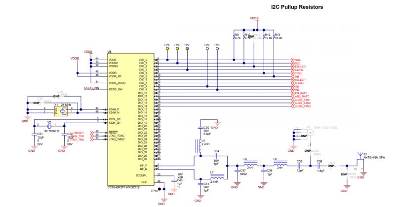
CC2640R2F: 2.4GHz low energy Bluetooth with ultra-low power wireless MCU (32-bit Arm Cortex-M3 processor).
TPS62745: Ultra-low IQ step-down converter with 16 selectable output voltages (1.8V to 3.3V) and 90% efficiency (when load current ≥15μA).
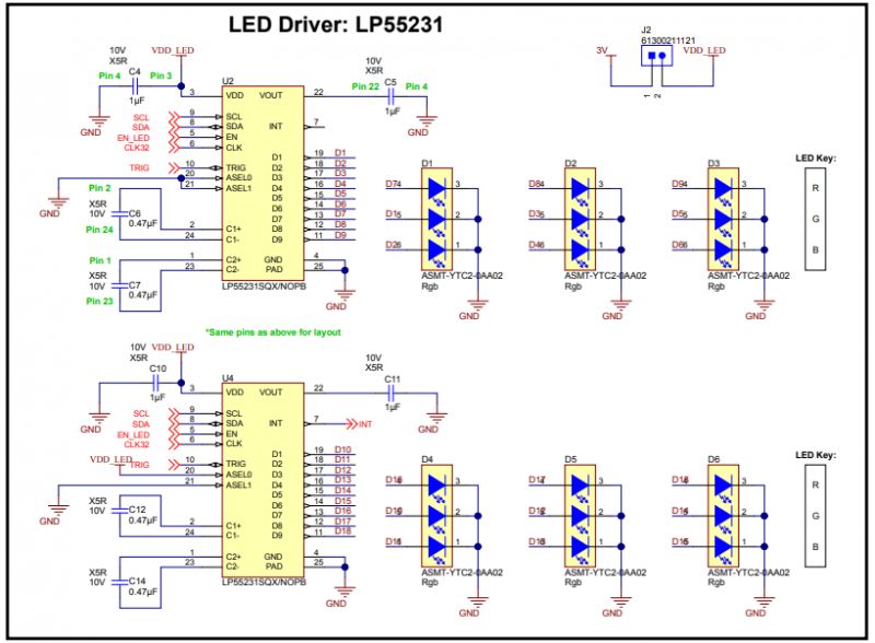
LP55231: Nine-channel LED driver for making lighting effects for mobile devices.
CSD25310Q2: Low-cost power PFET with ±8V gate-source voltage and 19mΩ low RDSon.
TPD1E10B06: Single-channel ESD with 10pF capacitance and 6V breakdown voltage in 0402 package.
The above core devices are sold in Huaqiang Core City. For more information, please click "Read the original text" and log in to Huaqiang Core City to view.
The following figure shows the BOM material list.

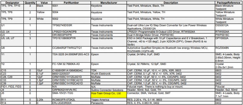
>>>To view the complete BOM list, please click "Read Original"
4. System circuit diagram
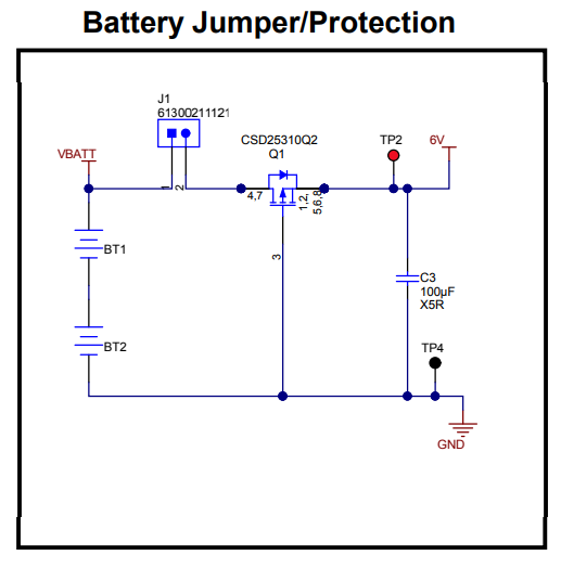
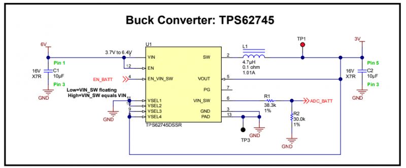


>>For complete circuit diagram, please click "read original text"
5. Hardware overview
The following figure is the hardware of the design. The PCB is a rectangle of 3.5 inches x 4.0 inches. However, no measures were taken during the development process to reduce its dimensions. The PCB is located on a 1-inch nylon pillar and can be easily used when performing laboratory measurements.
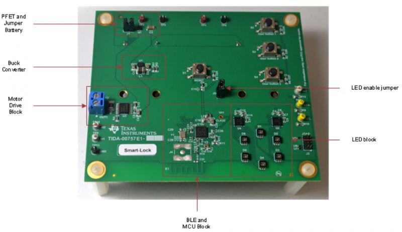
The board has two jumpers. Using J1 in the upper left corner of the board, the user can disconnect the battery from the rest of the reference design.
Using J1, the current measurement results can also be collected through the 6V power rail. J5 is located near the center of the board and connects the 3V power rail to the LED driver. The role of J5 is particularly prominent when there is no need to run the LED during the test.
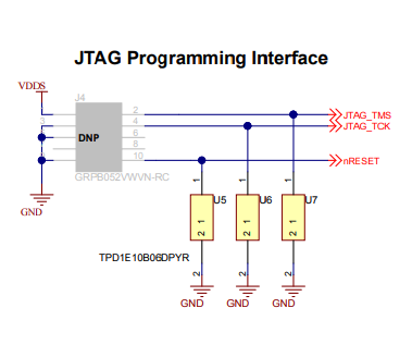
The lower left corner of the board contains the motor connection terminal block and test points as well as the DRV8833 motor controller. The I2C test point and the LED controller interrupt test point are located at the lower right corner of the board, near the JTAG programming connector.
The CC2640R2F and PCB antenna are located in the middle of the lower part of the board. Six RGB LEDs are arranged in a ring on the left side of CC2640R2F, and two LP55231 LED controllers are located above the LEDs.
The design also contains some buttons. The three user buttons are located in the upper right corner, and the reset button is located in the center of the board.
It is recommended to install the battery with J1 removed, and then install this jumper to power the circuit. After power up, all six LEDs flash pink immediately to notify the user that the device has been powered up correctly.
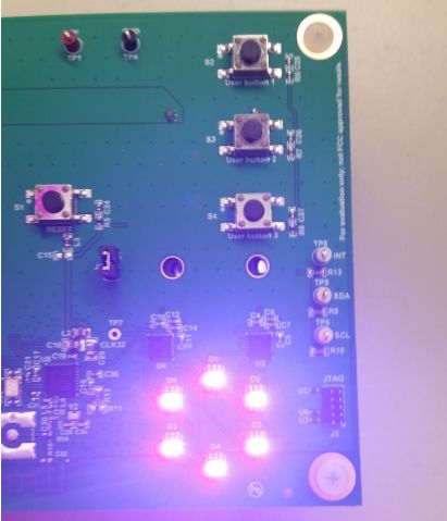
Pink start LED
When the Bluetooth connection device is not used, the user buttons (S2, S3, and S4) can activate different functions of the design. After pressing S2, a series of light changes will begin, and the six RGB LEDs will cyclically light up a variety of different colors. S3 drives the motor forward. The motor will stop after pressing S3 again or 10 seconds later. S4 drives the motor back. The motor will stop after pressing S4 again or 10 seconds later.
In order to communicate using Bluetooth, use an iOS app called LightBlue™ for testing. Other general Bluetooth applications can be used on various platforms. The function of the B-BLE application on Samsung®GalaxyS®6 has been tested.
6. PCB layout
The following figure shows the PCB layout of the smart lock design. In order to ensure high performance, this design uses a 4-layer PCB layout. The second layer is a solid ground layer, and the third layer is used for power rail wiring (no ground fill).
The top and bottom layers are used for general signal wiring, and the unused area is also filled with ground. We place the onboard Bluetooth antenna as far away as possible from other noise sources, including buck converters or other components that can act as antennas (such as test points or large traces).

Jiangmen Hongli Energy Co.ltd , https://www.honglienergy.com