How to use FPGA technology to solve DSP design problems?
DSP is very important for electronic system design because it can quickly measure, filter or compress real-time analog signals. This helps to realize the communication between the digital world and the real (analog) world. However, as electronic systems become more refined, multiple analog signal sources need to be processed, forcing engineers to make difficult decisions. Is it more advantageous to use multiple DSPs and synchronize their functions with the rest of the system? Or is it more advantageous to use a high-performance DSP with sophisticated software that can handle multiple functions?
Because today's systems are very complex, in many cases, a single DSP implementation simply does not have enough processing power. At the same time, the system architecture cannot meet the cost, complexity, and power consumption requirements of a multi-chip system.
FPGA has become an ideal choice for systems that require high-performance DSP functions. In fact, compared with a standalone digital signal processor, FPGA technology can often provide a greatly simplified solution for difficult DSP challenges. To understand the reason, you need to review the origin and development of DSP.
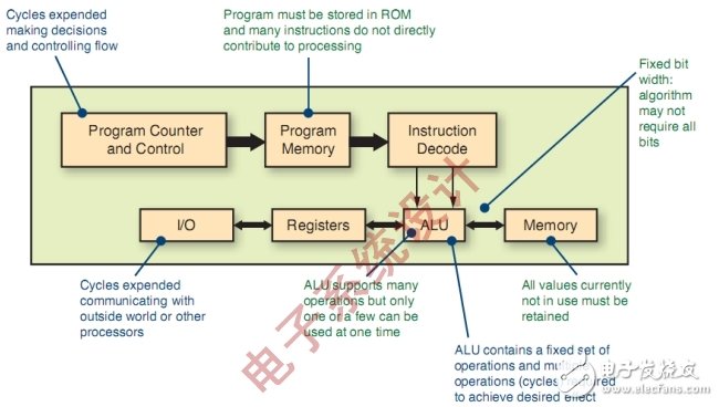
Figure 1: Traditional DSP architecture.
Dedicated microprocessor
In the past two decades, traditional DSP architectures have been doing their best to keep up with the ever-increasing performance demands. But as the video system strides into the era of high-definition and 3D, and the communication system has used the existing technology to the extreme in order to achieve higher bandwidth, designers need alternative implementation strategies. The hardware commonly used to implement digital signal processing algorithms is nothing more than one of the following three basic devices: microprocessors, logic circuits, and memories. Part of the design also requires additional hardware to implement analog-to-digital (A/D) and digital-to-analog (D/A) conversion and high-speed digital interfaces.
The traditional digital signal processor is a microprocessor designed to achieve a special purpose. This type of processor is very suitable for algorithm-intensive tasks, but its performance is limited by the clock rate and the order of its internal design. This limits the maximum number of operations they can perform per second on input data samples. Generally speaking, each execution of an arithmetic logic unit (ALU) operation requires three or four clock cycles. Multi-core architecture can improve performance, but the improvement is still limited. Therefore, the traditional signal processor design must reuse the architectural unit for algorithm implementation. For each execution of addition, subtraction, multiplication or any other basic operations, whether it is internal or external feedback, each execution must loop through the ALU.
Unfortunately, when dealing with today's numerous high-performance applications, this traditional DSP is difficult to meet the requirements of the system. Various solutions have been proposed in the past for this, including using multiple ALUs in one device, or arranging multiple DSP devices on a board. However, these programs often cause a substantial increase in costs, and only push the problem to another area. For example: using multiple devices to improve performance follows an exponential curve. To double the performance, two devices are required. To double it again, four devices are required, and so on. In addition, programmers often shift from focusing on signal processing functions to focusing on task scheduling between multiple processors and cores. This will generate a lot of additional code, and these codes will become system overhead, rather than used to solve the immediate digital signal processing problems.
The introduction of FPGA technology has brought good news for solving the increasing complexity of DSP implementation. FPGA was originally developed to integrate and centralize discrete memories and logic circuits to achieve higher integration, better performance, and higher flexibility. FPGA technology has become an important part of almost every high-performance system in use today. Compared with traditional DSP, FPGA is a huge parallel structure composed of a unified array composed of configurable logic block (CLB), memory, DSP logic slice (Slice) and some other components. They can be programmed using high-level description languages ​​such as VHDL and Verilog, or they can be programmed in a block diagram using System Generator. FPGA also provides numerous dedicated functions and IP cores for directly completing implementation schemes in a highly optimized manner.
The main advantage of digital signal processing in FPGA is the ability to customize the implementation according to system requirements. This means that for multi-channel or high-speed systems, users can make full use of the parallelism of FPGA devices to optimize performance, while for low-speed systems, more serial methods can be used to complete the design. In this way, designers can customize the implementation according to the requirements of the algorithm and the system, without having to compromise the desired ideal design to cater to the many limitations of pure sequential devices. In addition, ultra-high-speed I/O can further reduce costs and reduce bottlenecks by maximizing the data flow from the capture and processing chain to the final output.
The following takes a FIR filter implementation scheme that uses both traditional DSP architecture and FPGA architecture as an example to illustrate the pros and cons of each solution.
Digital FIR filter example
Finite impulse response (FIR) filters are one of the most widely used digital signal processing components. Designers use filters to change the amplitude or frequency spectrum of a digital signal, usually to isolate or highlight specific areas in the sample data spectrum. From this perspective, the filter can be regarded as a signal preprocessing method. In a typical filter application, input data samples are combined with filter coefficients through carefully synchronized mathematical operations (depending on the type of filter and implementation strategy), and then the data samples enter the next processing stage. If the data source and destination are both analog signals, the data samples must first pass through the A/D converter, and the result must be fed to the D/A converter.
The simplest type of FIR filter is implemented using a series of delay elements, multipliers and adder trees or adder chains.
The following equation is the mathematical expression of a single-channel FIR filter:
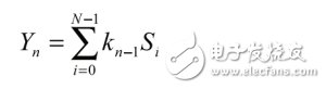
The terms in the equation represent input samples, output samples, and coefficients, respectively. Assuming that S is a continuous stream of input samples, and Y is a stream of output samples generated after filtering, then n and k correspond to a specific instantaneous time. In this way, if you want to calculate the output sample Y(n) at time n, you need a set of samples at N different time points, namely: S(n), S(n-1), s(n-2), …S(n-N+1). Multiply the set of N input samples by N coefficients and sum them to get the final result Y.
Figure 2 is a block diagram of a simple 31-tap FIR filter (length N=31).
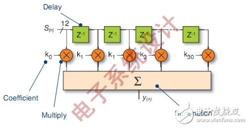
Figure 2: FIR filter with a length of 31 taps.
When choosing the ideal length and coefficient value of the filter, there are a variety of design tools available. Its purpose is to achieve the desired filter performance by selecting appropriate parameters. The most commonly used design tool for parameter selection is MATLAB. Once the filter parameters are selected, they can be implemented using mathematical equations.
The basic steps to implement FIR filters include: sampling the input data stream; organizing the input samples in the buffer so that each captured sample is multiplied by each filter coefficient; each data sample is multiplied by each coefficient , And accumulate the result; output the filtering result.
A typical C language program that uses "multiply and accumulate" to implement FIR filters on a processor is shown in the following code:
/*
*Capture input data samples
*/
datasample=input();
/*
*Load new data samples into the buffer
*/
Sï¼»nï¼½=datasample;
/*
*Multiply each data sample with each coefficient and accumulate the result
*/
y=0;
for(i=0;i{
y+=k[i]*S[(n+i)%N];
}
n=(n+1)%N;
/*
*Output filtering result
*/
output(y);
The implementation shown in Figure 3 is called a multiply-accumulate or MAC-type implementation. This is basically the way to implement a filter with a traditional DSP processor. The maximum performance of a 31-tap FIR filter implemented in this way using a typical DSP processor with a core clock rate of 1.2GHz is about 9.68MHz, or the maximum input data rate is 968MS/s.
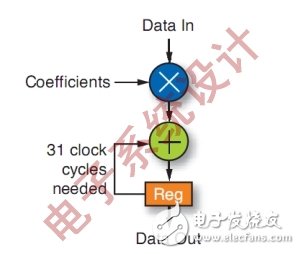
Figure 3: MAC implemented with traditional DSP.
And FPGA provides many different implementation and optimization options. If high resource efficiency is required, the MAC engine law is quite ideal. Still take the 31-tap filter as an example to illustrate the influence of the filter specification on the required logic resources. The block diagram of this implementation scheme is shown in Figure 4.
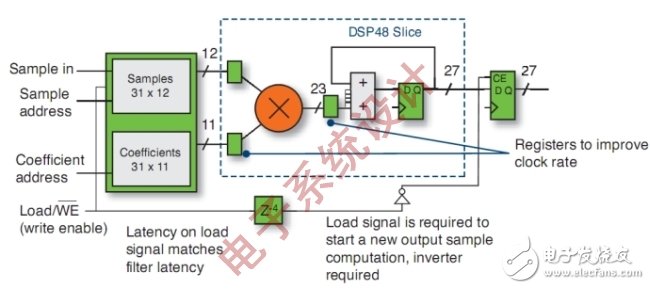
Figure 4: MAC engine FIR filter implemented by FPGA.
This design requires a memory to store data and coefficients, and RAM and ROM inside the FPGA can be mixed. RAM is used to store data samples, so a cyclic RAM buffer is used. The number of words is equal to the number of filter taps, and the bit width is set according to the sample size. ROM is used to store coefficients. In the worst case, the number of words is equal to the number of filter taps, but if there is symmetry, the number of words can be reduced. The bit width must be sufficient to support the largest coefficient. Because the data samples and coefficient data change with each cycle, a full multiplier is required. The accumulator is responsible for accumulating the results produced. Because the output of the accumulator changes with each clock cycle as the filter collects data, a capture register is required. When a full set of N samples are accumulated, the output register is responsible for capturing the final result.
If the MAC mode is used, DSP48 is very suitable, because the DSP48 Slice contains input registers, output registers and adder units. The resources required to implement the 31-tap MAC engine include a DSP48, an 18kb block RAM (block RAM) and 9 logic slices. In addition, some logic slices are needed for sampling, coefficient address generation and control. If the FPGA has a built-in 600MHz clock, in a Xilinx 7 series device with a -3 speed grade, the filter can run at an input sampling rate of 19.35MHz or 1,935MS/s.
If the system specification requires a higher-performance FIR filter, it can be implemented in a parallel structure. Figure 5 shows a block diagram of the direct type I implementation.
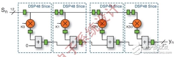
Figure 5: Direct Type I FIR filter implemented with FPGA.
The direct I-type filter structure can achieve the highest performance in the FPGA. This structure (usually referred to as a pulsating FIR filter) uses pipelines and adder chains to maximize the performance of the DSP48 Slice. The input is fed to the cascaded register used as a data sample buffer; each register provides a sample to the DSP48, which is then multiplied by the corresponding coefficient; the adder chain stores part of the product, and then adds them sequentially to get the final result.
This design does not require external logic circuits to support the filter, and the structure can be extended to support any number of coefficients. Because there is no high fan-out input signal, this structure can achieve the highest performance. Only 31 DSP48 logic slices are required to implement a 31-tap FIR filter. If the FPGA has a built-in 600MHz clock, in a Xilinx 7 series device with a -3 speed grade, the filter can run at an input sampling rate of 600MHz or 600MS/s.
From this example, it can be clearly seen that FPGA not only significantly surpasses the traditional digital signal processor in performance, but also the required clock rate is significantly reduced (therefore, the power consumption is also significantly reduced).
This example only reflects two technologies for implementing FIR filters using PFGA. In order to make full use of the data sampling rate specification, the device can be further customized. At this time, the data sampling rate can be selected between the extreme value of continuous MAC operation and the extreme value of fully parallel operation. Users can also consider making more trade-offs in terms of resource utilization and performance including symmetric coefficients, interpolation, decimation, multi-channel or multi-rate. Xilinx CORE Generator or System Generator utility tools can help users fully explore these design variables and technologies.
Choose between traditional DSP and FPGA
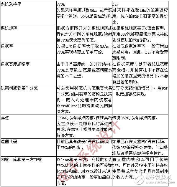
Traditional digital processors have been used for many years, and of course there are examples of providing the best solutions for specific problems. If the system sampling rate is lower than a few kHz and is implemented as a single channel, DSP may be the best choice. However, when the sampling rate increases above several MHz, or if the system requires multiple channels, FPGAs become more and more advantageous. Under high data rate conditions, DSP may only be able to collect, process and output data without causing any loss. This is because there are a large number of shared resources, buses and even cores in the processor. However, FPGAs can provide dedicated resources for each function.
DSP is an instruction-based rather than a clock-based device. Generally speaking, three to four instructions are required for any mathematical operation on a single sample. The data must first be collected by the input, and then sent to the processing core. After each operation is completed, it will circulate through the core and then be sent to the output. In contrast, FPGAs are clock-based, so it is possible to perform a mathematical operation on the input data stream every clock cycle.
Because the operation of DSP is based on instructions or codes, the programming mechanism is standard C language, or low-level assembly language is used when higher performance is required. This kind of code may contain advanced decision trees or transfer operations, which are difficult to implement in FPGAs. For example: there is a large amount of legacy code used to perform predefined functions or standards such as audio and telephony codecs.
FPGA manufacturers and third-party partners have realized the advantages of using FPGAs for high-performance DSP systems, and many IP cores are now widely used in most vertical application markets such as video, image processing, communications, automotive, medical, and military applications. Compared with the DSP design that maps the block diagram of the high-level system into C language code, it is easier and easier to decompose the block diagram of the high-level system into FPGA modules and IP cores.
From DSP to FPGA
Examining some of the main criteria will facilitate the decision-making between traditional DSP and FPGA (Table 1).
It is an indisputable fact that the number of software programmers far exceeds the number of hardware designers. The same is true for the relationship between the number of DSP programmers and the number of FPGA designers. However, it is not as difficult for system architects or DSP designers to Switch to FPGAs as it is for software programmers to switch to hardware design. There are a lot of resources that can significantly ease the learning process of DSP algorithm development and FPGA design work.
The main obstacle is the shift from a sample and event-based approach to a clock-based problem description and solution. If it can be completed in the system architecture and definition phase of the design process, the understanding and application of this conversion will be much simpler. It is common for different engineers and mathematics experts to define the system architecture (DSP algorithm and FPGA design are isolated from each other to some extent). Of course, if each member has a certain degree of understanding of the problems faced by other team members, the process will be much smoother.
Heating Element Temperature Control,Electric Grill Temperature Controller,Thermostat For Heating Element,Oven Capillary Thermostat
Foshan City Jiulong Machine Co., Ltd , https://www.jlthermostat.com