Class D audio amplification solution A7013 solves the problem of multimedia mobile phones
Loudspeaker damage due to high gain changes
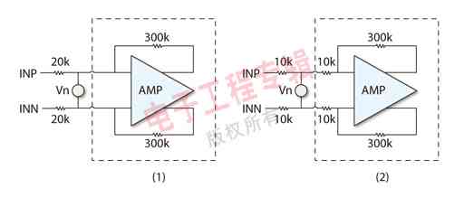
The mono class D power amplifier commonly used on mobile phones uses an external output resistor (see Figure 1) to adjust the gain. Due to the gain error, the speaker is damaged. This problem has gradually attracted the attention of mobile phone manufacturers. Recently, many well-known domestic mobile phone manufacturers have feedback that the use of large gain mono Class D amplifiers in the design of mobile phones, end customers play sound at high volume, and long-term use may damage the speakers, even if they are replaced by foreign manufacturers. Within other chips, the problem has not been significantly improved. Later, the A7013 Class D amplifier from Apexon Microelectronics was used, and the repair phenomenon dropped by nearly 80%.
As we all know, it is difficult to obtain a resistor with an accurate absolute value in a semiconductor process. The rate of change in the absolute value of polysilicon resistors commonly used is ± 20%, while the absolute value of external resistors is relatively accurate. Therefore, when the customer works with a large gain, the gain is easily shifted out of the maximum power range of the speaker, thereby causing damage to the speaker. In the semiconductor process, it is easy to obtain the accuracy of matching the relative value of the resistance. The deliberate matching layout can easily reach the matching accuracy of 0.1%. We can use this to avoid the gain offset caused by the internal resistance offset. The specific scheme is as follows:

Figure 1 Traditional gain setting, Figure 2 Improved gain setting
Option 1: As shown in Figure 2, while ensuring that the external gain is controllable, the on-chip 10k input resistance is retained. (The following assumes that the off-chip resistance will not have an absolute value deviation)
Assuming that the internal resistance of the 300k chip in Figure 1 is shifted by 20%, the gain will be shifted by 20%, and the normal gain of 15 times will be shifted by 12 to 18 times, so the power will exceed the rated power.
Gainmax = 300 × 120% / 20 = 18 = 15 × (1 + 20%)
Gainmin = 300 × 80% / 20 = 12 = 15 × (1-20%)
If the improved gain setting shown in Figure 2 is used, assuming that the 300k resistor is offset by 20%, the internal 10k resistor will also be offset by 20% (due to the matching accuracy of 0.1%).
Gainmax = 300 × 120% / (10 + 10 × 120%) = 16.36 = 15 × (1 + 9.1%)
Gainmin = 300 × 80% / (10 + 10 × 80%) = 13.33 = 15 × (1-1.11%)
Therefore, in the improved scheme, the maximum gain offset is 9.1%, and the minimum gain offset is 11.1%, which is much lower than the 20% offset level before the improvement.
Option II:
By sacrificing the chip yield rate, the chip is screened to a resistance drift of 10%, and the improved method will also obtain a more accurate gain limit, thereby avoiding speaker damage caused by large shifts in the gain of mobile phone manufacturers.
third solution:
The product can also be realized by automatic gain control (AGC) to avoid burning the speaker at high power. But this kind of scheme usually costs a lot.
It can be seen that for Class D power amplifier IC design companies, the first solution will not increase the cost, and when applied by mobile phone manufacturers, it can also avoid the phenomenon of speaker frequency damage due to gain offset. A7013 combines the advantages of solution one and solution two, and is the only successful and mature solution among similar products.
In addition, for the problem of speaker damage, by studying the response frequency band of the mobile phone speaker, it can be found that the mobile phone speaker can only respond to the frequency band above 300Hz, which causes the power of the frequency band below 300Hz to be lost as heat. Changing the input capacitance can change the input signal bandwidth, filter out the frequency band power that cannot be responded to by the speaker, thereby reducing the peak power and also affecting the reliability of the speaker.
The scheme given in Figure 2 also has certain advantages for improving noise interference. In Figure 1, if the customer's layout is not careful and weak noise is coupled to the input of the op amp, the noise will be amplified by the multiple of the open loop gain of the op amp (tens of thousands of times), and audible coupling will appear in the speaker noise. With the scheme in Figure 2, as long as the chip internally considers the input of the op amp, the weak noise introduced at the external input pin can only be amplified by a few tens of times, which greatly facilitates the customer's layout in this part.
Improve amplifier sound
In recent years, the general impression of class D amplifiers is high power efficiency and poor sound quality. For the sound quality of class D amplifiers, there has been debate in the industry. Apexon A7013 uses an independent patented enhanced feedback architecture (EFS) to improve class D amplifiers. Sound quality. While achieving high power efficiency, it also greatly improves the distortion of Class D amplifiers, thereby giving Class D amplifiers great advantages in terms of sound quality and efficiency.
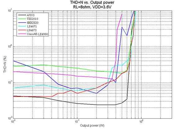
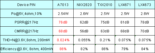
As shown in Figure 3 and Table 1, it can be seen that EFS technology improves the distortion of Class D amplifiers. The A7013 distortion using EFS technology is the lowest in the entire power range; at the same time, due to the improvement of high power THD + N, A7013 distortion is less than 1% It also has outstanding performance in terms of maximum power.

Fig. 3 adopts EFS scheme to improve THD + N. (The data quoted in the figure are from the product data sheet)

Table 1 Other performance improvements using the EFS scheme. (The data quoted in the table are all from the corresponding product data sheet)
Apexon Class D amplifier A7013 maintains its high efficiency and low distortion, while considering the customer's specific application problems, providing a complete solution in terms of reliability and performance. A7013 is available in WCSP9 and DFN8 packages, and has been widely used by mobile phone design manufacturers and brand customers.

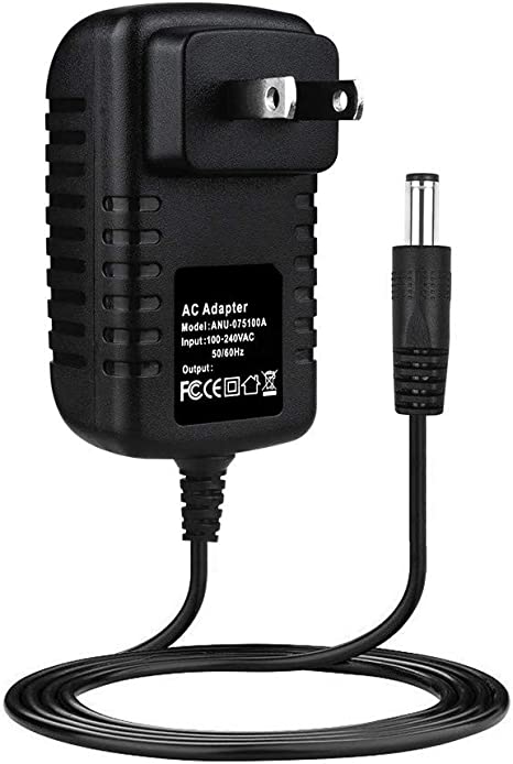
AC wall 5V 2A power adapter with multiple tips works for many small 5V electronics. Like Scanner, Router, Bluetooth speaker, Foscam Wireless IP Camera, CCTV camera, USB hub, bluetooth GPS Receiver, tv box, tablets, Baby Monitor, Graco Swing, Home Phone System, VoIP Telephone Routers, Serato DJ Controller, DVR, ADSL Cat, External battery, hubs, switches, Led Strip, String Lights, vibrator, Raspberry pi 3 Raspberry Pi A/A+/B/B+ Raspberry Pi Zero and more 5V devices. (5V ONLY)
Worldwide Input: 110-240V; Output: 5V 1000mA, 1.5A, 1.75A, 5V 1A, 5V 500mA, 5V 2.1A, Max 10W. DC Tip Polarity: Central Positive(+). Please read manual carefully before using 5vdc power supply.
Design-safeguard features against incorrect voltage, short circuit, internal overheating and overloading. This 5v Ac power supply charger is made from quality material to ensure the long lifetime. Power your 5v electronics perfectly and replaces lots of 5 volt power chargers
Package include: 1 x High Quality 5V 2A AC DC Power Adapter, 1 Set x Tips
5V Switching wall charger 6V Switching wall charger 9V Switching wall charger 12V Switching wall charger 15V Switching wall charger 19V Switching wall charger 24V Switching wall charger 36V Switching wall charger 48V Switching wall charger
Shenzhen Waweis Technology Co., Ltd. , https://www.waweisasdapter.com