7 steps to remove PBGA package from PCB
PBGA is a form of packaging. The main distinguishing feature is the use of an array of solder balls to make contact with a substrate such as a PCB. This feature allows PBGA to have different advantages over other pin configurations such as single-row, dual-in-line, and quad-column. This allows for higher pin densities. The interconnects inside the PBGA package are implemented by wire bonding or flip chip technology. PBGA chips containing integrated circuits are packaged in a plastic material.
Figure 1. PBGA device schematic
PBGA Device Rework After mounting the PBGA device on the PCB, if a defect is found, it should be repaired to remove the defective device and replace it with a working device. Before removing the device, the bad device should be heated until the solder joint is liquefied to remove the defective device from the circuit board.
Routine repair procedures are as follows
ⶠPrepare the board
移除 Remove the device
æ¸…æ´ Clean PCB pads
涂敷 Coating paste
器件 Device Alignment and Patching
固定 Fixed devices
â¼ Check
Before describing the above seven steps, let's talk about removing the device and layering the attention.
Mechanical stress on the PBGA and/or PCB may occur when the device is removed. Care should be taken to remove bad components to avoid damaging the PCB, adjacent devices, and bad components themselves, especially if the user intends to perform fault analysis on the bad component.
Excessive stress on the PBGA device, such as heating the device above the rated peak temperature or overexposure to high temperatures, may result in delamination of the package or external physical damage (see Figures 2 and 3). For devices to be further analyzed, the layering caused by improper removal will increase the difficulty of finding the true fault mechanism. Therefore, in order to perform effective fault analysis, it is necessary to properly remove the defective devices.
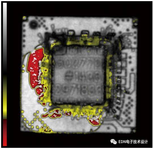
Figure 2. Overheating causes delamination between the substrate and the molding material of a PBGA device (observed by a scanning acoustic microscope)
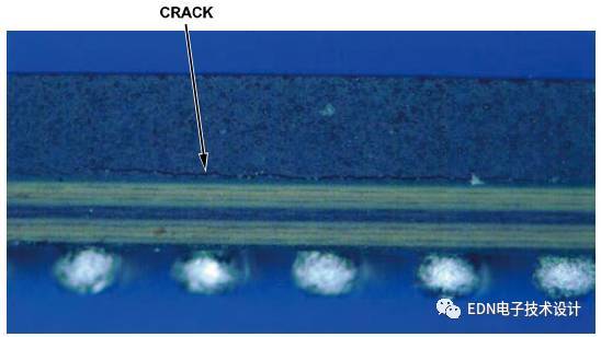
Figure 3. Low-magnification image of cracks on PBGA caused by overheating (side view)
Prepare the board
It is strongly recommended that the PCB assembly be dry-baked before rework to eliminate residual moisture. If not eliminated, residual moisture may damage the device due to the "popcorn effect" during reflow. Bake PCB components at 125°C for at least 4 hours as long as these conditions do not exceed the rating limits of other devices on the PCB. If these conditions exceed the rating limits of other devices, the alternative baking conditions described in the joint industry standard IPC/JEDEC J-STD-033 should be used.
Remove the device
Different tools can be used to remove the device. To remove the device, it may be necessary to heat the device until the solder reflows and then remove the device mechanically while the solder is still in the liquid state. The programmable hot air rework system provides controlled temperature and time settings. The temperature curve used for device assembly should be followed during repairs. The return temperature must not exceed the peak temperature specified on the humidity sensitivity level (MSL) label. The heating time can be shortened (for example for the liquefaction zone) as long as complete reflow of the solder is achieved. The solder reflow zone should be at a peak temperature of less than 60 seconds. The vacuum pressure of the pick-up tool should be less than 0.5 kg/cm2 to prevent the device from ejecting before it reaches full reflow and to avoid the pad floating away. Do not use the device removed from the PCB.
Control the rework temperature to prevent damage to the PBGA device and PCB. It should be considered that because of the difference in thermal mass, PBGA can be heated faster than lead frame-based packages, such as standard outline integrated circuit (SOIC) and lead frame chip scale package (LFCSP). Note that covering the area around the device with a heat-resistant tape provides further protection. In addition, it is recommended to heat the bottom of the PCB to reduce the temperature difference between the upper and lower sides of the PCB to minimize board bending.
When defining the rework tool settings, the temperature curve should be calibrated. This calibration is particularly important when you are reworking a particular device for the first time. PBGA devices also need to be calibrated with different body sizes, solder compositions, or different PCB materials, configurations, sizes, and thicknesses because they may have different thermal mass values.
The calibration must include monitoring of temperature, time, and other settings of the equipment tool (see Figure 4). Thermocouples should be mounted to different parts of the board assembly, such as the top of the PBGA device and the top of the PCB (see Figure 5). Analyze the time and temperature profile data and obtain valid parameters for device removal from the evaluation.
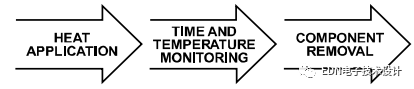
Figure 4. Simplified flow chart for device removal evaluation
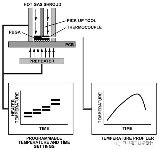
Figure 5. Device Removal Calibration Setup
Clean PCB pads
After removing the PBGA device, the pads on the PCB have too much solder and must be cleaned before the PBGA device is replaced. Pad cleaning can be divided into two steps:
Go to tin. Remove excess solder from the pads using a solder wire and blade solder (see Figure 6). The width of the selected blade should match the maximum width occupied by the device. The blade temperature must be low enough to avoid damaging the board. Solder can be applied to the pad and excess solder can be removed with a solder wire and soldering iron.
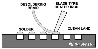
Figure 6. Detaching of PCB pads
clean. Clean with a cleaning agent on the return area and clean it with a lint-free cloth. The cleaning agent used depends on the type of solder paste used in the original assembly.
Coating paste
The solder paste should be applied prior to mounting the replacement PBGA device on the circuit board in order to replace the solder paste applied when the circuit board was originally assembled, thus ensuring the reliability of the PBGA solder joint. The amount of solder paste applied to each solder ball must be the same so that there is no coplanarity when PBGA is mounted on the circuit board.
The template can be used to apply solder paste to PCB pads. Template alignment accuracy is the key to maintaining uniform solder reflow processing. Uses the same PBGA aperture geometry and stencil thickness as the board assembly. Use a trapezoidal aperture (see Figure 7) to ensure uniform paste release and reduce smearing.
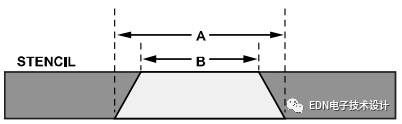
Figure 7. Template aperture geometry (A is longer than B)
In some cases, it may not be feasible to use the template to evenly and accurately apply the solder paste on the PCB pads, especially for circuit boards with high device density or geometric space. In this case, consider applying solder paste to the solder balls on the bottom of the device. For this purpose, solder paste can be applied to the upper end of the solder ball using a template, or solder paste can be dispensed to all solder balls (see FIGS. 8 and 9). Specially designed fixtures and/or rework equipment can be used for this purpose.
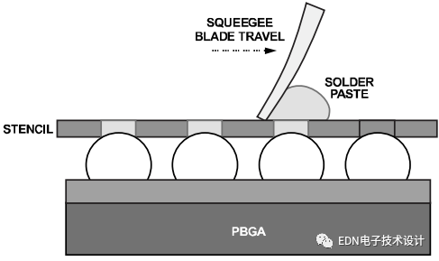
Figure 8. Solder paste template to print solder paste onto solder balls
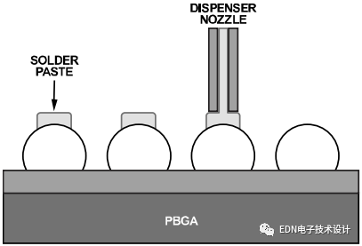
Figure 9. Solder paste dispensed on solder balls
Device alignment and patching
It is important to accurately place the device on the circuit board. SMT devices with split beam optics help align the PBGA and the board. This type of imaging system involves superimposing PBGA solder balls on the PCB pad image (see Figure 10). The placement machine must have the ability to support user fine-tuning (including rotation) along the x-axis and y-axis.
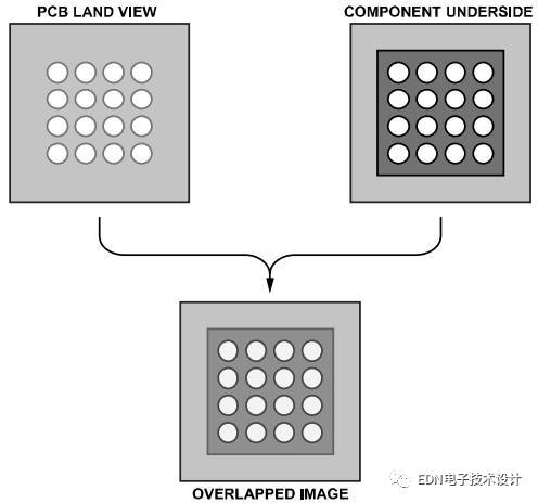
Figure 10. Alignment of PCBs and Devices Using Split Beam Optical Systems
The accuracy of the patch depends on the equipment or process used. Although PBGA packages tend to align automatically during solder reflow, it should be ensured that the patch deviation is less than 50% of the PCB pad width. If the alignment error is too large, the solder bridging may cause an electrical short circuit.
Fixed device
Since all reflow parameters are optimized, the heat curve developed during the original assembly process should be used.
an examination
After reflow, check the assembled PBGA for defects such as misalignment or damage. Use X-rays to check for problems such as solder bridging and solder balls. If necessary, perform an electrical verification test to verify that the device is functioning properly.
PLC, that is, planar optical waveguide, that is to say, the optical waveguide is located in a plane.
As everyone is familiar with single-layer circuit boards, all circuits are located in a plane of the substrate. Therefore, PLC is a kind of technology, it does not refer to a certain type of product, let alone a splitter! Our most common PLC splitter is made of silicon dioxide (SiO2). In fact, PLC technology involves a wide range of materials, such as glass/silicon dioxide (Quartz/Silica/SiO2), lithium niobate (LiNbO3), III-V semiconductor compounds (such as InP, GaAs, etc.), silicon-on-insulator (SOI/SIMOX), silicon oxynitride (SiON), polymer, etc.
Devices based on planar optical waveguide technology solutions include: Splitter, Star coupler, Variable Optical Attenuator (VOA), Optical switch, Optical comb ( Interleaver) and Array Waveguide Grating (AWG), etc. According to the requirements of different applications (such as response time, ambient temperature, etc.), these devices can be made by choosing different material systems and processing techniques. It is worth mentioning that these devices are all optical passive devices and are independent. They can be combined with each other or with other active devices to form high-end devices with different functions.
Optical Fiber, ABS BOX PLC splitter,Fiber Cable Splitter
Shenzhen GL-COM Technology CO.,LTD. , https://www.szglcom.com