Analysis of lcd1602 timing diagram
Operational timing is always used as the most important part of any IC chip. All usage details of a chip are included in its official device manual. So the first thing to do well with a device is to extract and master the useful content of its device manual.
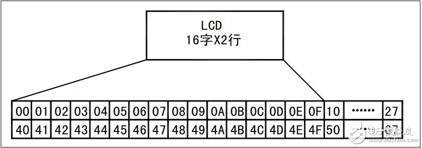
Lcd1602 is an industrial character LCD that can display 16x02 or 32 characters at the same time. Lcd1602 liquid crystal display principle lcd1602 liquid crystal display principle is to use the physical characteristics of liquid crystal, through the voltage to control its display area, there is electricity display, so that you can display the graphics.
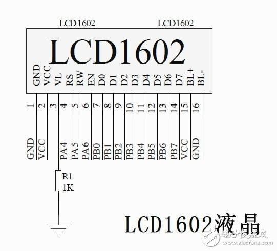
Timing diagram 3: VL, liquid crystal display bias signal, used to adjust the display contrast of lcd1602, generally external potentiometer to adjust the bias signal, note that this pin voltage is 0 to get the strongest contrast.
Timing diagram 4: RS, data/command selection. When this pin is high, the data byte can be transferred to 1602. When this pin is low, the command byte is transmitted. The command byte, which is the byte used to set some of the working modes of lcd1602; the data byte, even if it is used to display the byte on 1602. It is worth mentioning that the data of lcd1602 is 8-bit.
Timing diagram 5: R/W, read and write selection. When this pin is high, the data operation can be performed on the lcd1602, and vice versa.
Timing diagram 6 pin: E, enable signal, is actually the data control clock signal of lcd1602, using the rising edge of the signal to achieve data transmission to lcd1602.
Timing diagram 7~14: 8-bit parallel data port makes data reading and writing to lcd1602 very convenient.
Lcd1602 operation write timing diagram
1. When we want to write the instruction word and set the working mode of lcd1602: we need to set RS to low level, RW to low level, then send the data to data port D0~D7, and finally the E pin has a high pulse. Write data.
2. When we want to write the data word, realize the display on lcd1602: we need to set RS to high level, RW to low level, then send the data to data port D0~D7, and finally the E pin is high. The pulse writes the data.
Lcd1602 operation read timing diagram
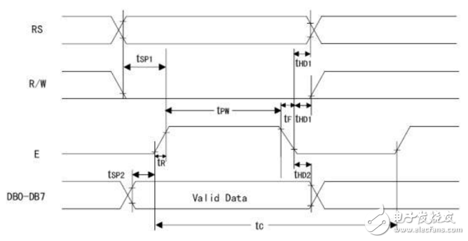
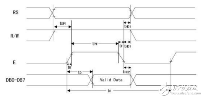
1. Pay attention to the timing diagram timeline. If it is not marked (in fact, most of the timing diagrams are also not marked), then the direction from left to right is the time forward axis, that is, the time is increasing.
2, understand some of the common sense required for the timing diagram:
(1) The leftmost part of the timing diagram is generally the identifier of a certain pin, indicating that the line of the line reflects the change of the pin.
(2) The timing diagram is a portion that is wired and intersected, indicating that the level is changing.
(3) The two parallel lines respectively correspond to the high and low levels, which also coincides with the statement that the level changes in (2).
(4) The diamond part of the lower part of the figure is sealed. Note that the data is valid, and the word Valid Data also shows this.
3, look at the timing diagram needs to be very serious attention is that the timing of each pin in the timing changes, the timeline based on the timing diagram is consistent. It is important to accurately observe the timing diagram in strict accordance with the growth direction of the timing diagram timeline. Let the device strictly follow the changes in the timing diagram. This is particularly critical in a single bus device like the 18B20.
4, the above points, not unique to the timing diagram of lcd1602, most of the timing diagrams follow such general rules, so we should get used to such rules.
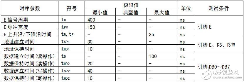
Perhaps you have also noticed that the timing diagram above has a lot of time-specific annotations, which is also very important information. The annotations at these times indicate the shortest or longest time that certain states are to be maintained. Because the operating speed of the device is also limited, generally can not keep up with the speed of the master chip, so they must have a timing coordination directly.
Semiconductor Parts
Semiconductor Parts
YANGZHOU POSITIONING TECH CO., LTD. , https://www.cnpositioning.com