Basic concept of clock jitter (Jitter)
As the clock rate in communication systems moves into the GHz class, jitter, a key factor in analog design, is beginning to gain increasing attention in the digital design arena. In high speed systems, the timing error of the clock or oscillator waveform limits the maximum rate of a digital I/O interface. Not only that, it also leads to an increase in the bit error rate of the communication link and even limits the dynamic range of the A/D converter. It has been shown that in systems above 3 GHz, jitter can cause inter-symbol interference (ISI), resulting in an increase in transmission error rate.
1 basic concept of clock jitter (Jitter)
Jitter is defined as "the deviation between the timing event of the signal and its ideal position." The description in the SONET SPEC is: Jitter is defined as the short-term variations of a digital signal's significant instants from their ideal positions in time.
Ideally, a perfect pulse signal with a fixed frequency (in the case of 1MHz) should have a duration of exactly 1us with a transition edge every 500ns. But unfortunately, this signal does not exist. As shown in Figure 1, the length of the signal period will always change, resulting in an indeterminate arrival time for the next edge. This uncertainty is jitter.
Jitter is a measure of the time domain variation of a signal. It essentially describes how much the signal period deviates from its ideal value. In most literatures and specifications, time jitter is defined as the deviation of the arrival time of the high-speed serial signal edge from the ideal time, except that in some specifications, the component that changes slowly in this deviation is called time. Wander, and define the faster component as time jitter.
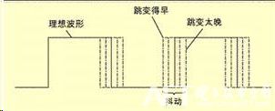
Figure 1 Schematic diagram of time jitter
2 classification of clock jitter
There are two main types of jitter: deterministic jitter and random jitter.
Deterministic jitter is caused by identifiable interfering signals, which are usually of limited magnitude, have specific (rather than random) causes, and cannot be statistically analyzed.
Random jitter refers to timing changes caused by factors that are difficult to predict. For example, temperature factors that can affect the mobility of semiconductor crystal materials can cause random variations in the carrier stream. In addition, variations in semiconductor processing techniques, such as uneven doping density, can also cause jitter.
According to the calculation method of jitter, it can be divided into the following three types:
1) period jitter (period jitter)
Measure the width of each clock and data cycle in the real-time waveform. This is the earliest and most direct way to measure jitter. This indicator illustrates the change in the clock signal per cycle.
2) cycle-cycle jitter
Measure the variation of the period width of any two adjacent clocks or data. By applying a first-order difference operation to the period jitter, the inter-cycle jitter can be obtained. This indicator has obvious significance when analyzing the nature of the phase-locked loop.
3) Time interval error (TIE)
Measure how much each active edge of a clock or data deviates from its ideal position, using a reference clock or clock recovery to provide the ideal edge. TIE is particularly important in communication systems because it illustrates the cumulative effect of period jitter over various periods.
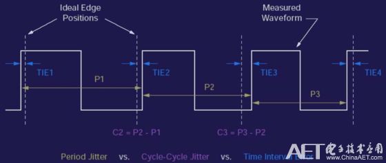
Figure 2 Schematic diagram of three kinds of time jitter
3 clock jitter calculation method
Example: A 100MHz clock, the first to fourth cycles are 9.9ns, 10.1ns, 9.9ns, 10.0ns, assuming that its ideal clock is fixed at 10ns.
TIE Jitter:
T1 = 10-9.9 = 0.1, T2 = 10-10.1 = -0.1, T3 = 10-9.9 = 0.1T4 = 10-10 = 0
TIE pk-pk jitter = 0.1 – (-0.1) = 0.2 ns
TIE RMS jitter = standard deviation of parameter T1..T4
Period Jitter
P1 = 9.9 P2 = 10.1 P3 = 9.9 P4 = 10
Period Jitter pk-pk value = 10.1 - 9.9 = 0.2 ns
Eriod Jitter RMS value = standard deviation of parameter P1..P4
Cycle to Cycle jitter
C1 = P2-P1 = 10.1-9.9 = 0.2 C2 = P3-P2 = 9.9-10.1 = -0.2C3 = P4-P3 = 10-9.9 = 0.1
Cycle to cycle jitter PK-PK value = 0.4 ns
Cycle to cycle jitter RMS value = standard deviation of parameter C1..C4
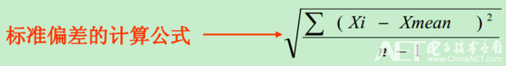
Figure 3 Standard deviation calculation formula
4 sources of clock jitter
4.1. Random jitter (RJ, Random Jitter)
Random jitter is temporal noise and does not have any known patterns. Although random jitter may have various probability distributions in the theory of stochastic processes, Gaussian normal distribution is usually assumed in the jitter model. There are two reasons for this. First, in many circuits, the main source of random noise is thermal noise, which has a Gaussian distribution. Second, according to the central pole limit law, many independent uncorrelated noise sources are superimposed and approximate a Gaussian distribution. Since the random jitter satisfies the Gaussian distribution, its peak is unbounded. This is an important feature that distinguishes random jitter from deterministic jitter.
4.2. Deterministic jitter (DJ, Deterministic Jitter)
Deterministic jitter (DJ) is a time jitter that can be repeated and predicted relative to random jitter. Therefore, the peak-to-peak value of DJ is bounded, and the position of this boundary can approach the true value as the number of measurements increases. DJs can be divided into several types, each with its own characteristics and the corresponding physical mechanism behind it.
1) Data Dependent Jitter (DDJ, Data Dependent Jitter)
Data-dependent jitter is the jitter associated with each bit of data. The reason for the usual DDJ is caused by inter-symbol interference (ISI) when the data stream passes through a channel with significantly limited bandwidth. The DDJ typically has two histograms in the form of discrete pulses, and the two peaks have the same height (which can be divided into high probability DDJ and low probability DDJ depending on where the peak is located).
2) Duty Cycle Distortion (DCD)
The duty cycle distortion jitter is the measurement jitter caused by the difference in the position of the zero crossing when the clock signal duty ratio is not 50%. There are two reasons for this. First, the slew rate of the rising edge of the signal and the slew rate of the falling edge are different. Second, the decision threshold is higher or lower. The DCD typically has two histograms in the form of discrete pulses similar to the DDJ, and the heights of the two peaks are the same.
3) Bounded uncorrelated jitter (BUJ, Bounded Uncorrelated Jitter)
Bounded uncorrelated jitter is a general term for time jitter that is not related to the jitter measurement time in time and has bounded peaks and peaks on the distribution. There are usually three sources: power supply noise. Due to the noise caused by the power supply, it may affect the bit error rate; crosstalk and external noise. Noise due to adjacent transmission lines or external electromagnetic interference during transmission; periodic noise. Periodic jitter due to various periodic noises (PJ, Period Jitter). For example: switching power supply noise or periodic signals used in testing. Only the periodic jitter (PJ) of a single frequency component has a histogram in which both ends are in the form of peak intermediate depressions.
5 analysis method of clock jitter
Due to the actual test, the composite time jitter often obtained is a combination of the above two or several Jitter models. Using the knowledge of probability theory, it can be known that the composite jitter probability density function is a convolution of the probability density function of the various random variables that make up the jitter. For example, a probability density function for DCD jitter and a random jitter is to modulate a random Gaussian distribution onto two peaks of the DCD. In addition, for periodic jitter (PJ), there are not only fundamental components, but also high-order harmonics.
5.1. Statistical properties and statistical histograms
Since all symbols containing jitter have random components, statistical calculations are widely used in the evaluation of jitter performance. Common statistical parameters include average value, standard deviation, maximum value, minimum value, peak-to-peak value, and so on. The histogram is usually used to visually describe these statistical characteristics of the jitter.
The abscissa of the statistical histogram is the size of the jitter, and the ordinate is the frequency at which the jitter appears within a certain interval. When the number of measurements is sufficient, the histogram is a good estimate of the probability density function of the jitter size, so the statistical histogram plays an important role when estimating the system error rate through jitter.
It should be noted that the histogram does not contain the sequence of occurrence of each jitter point, so it cannot be used to display the periodic information existing in the jitter.
5.2. Jiiter-time curve and frequency spectrum of Jitter
Since the statistical histogram does not show the modulation or periodic component information present in the Jitter, the Jitter-time curve can be used to describe the trend of the Jitter over time. The abscissa of the curve is the time at which the Jitter is measured, and the ordinate is the size of the Jitter. This way we can clearly see the pattern of Jitter changing with time from the picture.
Since Jitter has components that change over time, there is an obvious way to analyze the Jitter-time curve by Fourier transform to get the characteristics of its frequency domain.
5.3. Eye
So far, the eye diagram is still a qualitative and convenient method for analyzing digital communication, which can simultaneously give the amplitude information and time information of the transmission. The short segments of a series of waveforms are stacked together to align with the nominal edge position and voltage level. Once the jitter reaches +-0.5UI, the eyes will close and the receiver circuit will have a bit error.
It should be noted that the trigger source used when measuring the eye diagram should be a standard clock source with high frequency stability and low jitter, and its index directly affects the measurement accuracy. If you use the edge of the test signal to trigger directly, you need the oscilloscope to have a clock recovery function.
6 clock jitter measurement method
6.1. Oscilloscope measures Jitter
Jitter, which uses an oscilloscope to measure signals, first requires the oscilloscope to have sufficient bandwidth, signal-to-noise ratio, resolution, time accuracy, and signal fidelity to reduce the effects of measurement errors. The oscilloscope often uses software clock recovery to recover the ideal edge time (of course, an external high-quality clock source can be used as the ideal edge time), and the oscilloscope can generate an eye diagram by superposition. Through the analysis of the eye diagram, various parameters of the Jitter are obtained.
When using oscilloscope analysis, it is often necessary to do further Jitter analysis to get the nature of the error. At this time, the input data stream needs to be repeatedly transmitted according to a certain rule (usually using a pseudo-random sequence generator) to concentrate the energy of the DDJ component as much as possible. After collecting such a code stream waveform through an oscilloscope, the following analysis can be performed.
1) Interpolating the data obtained by sampling to recover the sampling waveform, and calculating the over-decision time of each edge for a certain decision level;
2) recovering the clock of the input signal by means of a software phase-locked loop, and calculating the jitter size of each edge respectively;
3) For a place where there is no edge such as 1 or even 0, the corresponding Jitter is obtained by linear interpolation;
4) Perform an FFT on the obtained Jitter-time function to obtain the spectrum of the Jitter.
Next, through the analysis of the Jitter spectrum, the corresponding peaks of DCD, DDJ, and PJ, and the noise floor of RJ can be found. Then separate the components to do IFFT to get the Jitter-time function of each component. The specific results here have a lot to do with the resolution of the FFT and the choice of the window function.
At present, many oscilloscope manufacturers provide analysis software for the oscilloscope, which can effectively decompose Jitter according to a certain model. For example, the TDS JIT3 from Tektronix is ​​the Jitter analysis suite for TDS5000 and above.
Of course, before doing complex Jitter analysis, it is recommended to use the traditional way - afterglow display to estimate the severity of Jitter:

The setup at this point is very simple, just use the cursor to measure the width of the edge of the waveform. However, it should be noted that pixel or screen resolution (quantization error) reduces accuracy; there is only a single waveform and trigger jitter is introduced.
Zoolied is able to produce various shapes of 45 degree beam splitter (filter) ,such as round, square, rectangle, Oval, Trapezoid as so on.
Thickness range from 0.2mm to 5mm.
Application of Zoolied Beam splitter plates:
Digital camera,
Machine vision,
Life science,
3D stereo light source,
Teleprompter,
Coaxial light source,
Biological microscope,
Optical fiber communication equipment,
Biological identification equipment.
Beamsplitter Plate,50/50 Beamsplitter Glass,Teleprompter Beam Splitter Plate,Beam Splitter Plate
Zoolied Inc. , https://www.zoolied.com