Basic principle analysis of Σ-Δ model ADC topology
The Σ-Δ ADC is an essential component in the toolbox of today's signal acquisition and processing system designers. The purpose of this article is to give the reader a basic understanding of the fundamentals behind the Σ-Δ model ADC topology. This article explores a trade-off analysis example of noise, bandwidth, settling time, and all other key parameters associated with ADC subsystem design to provide background information for precision data acquisition circuit designers.
It usually consists of two modules: a sigma-delta modulator and a digital signal processing module, which is usually a digital filter. A brief block diagram and main concepts of the Σ-Δ ADC are shown in Figure 1.
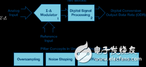
Figure 1. Key concepts of Σ-Δ ADC.
The sigma-delta modulator is an oversampling architecture, so we begin with Nyquist sampling theory and schemes and oversampling ADC operation.
Figure 2 compares the Nyquist operation of the ADC, the oversampling scheme, and the sigma-delta modulation (also oversampling) scheme.
Figure 2a shows the quantization noise when the ADC is operating in the standard Nyquist mode. In this case, the quantization noise is determined by the LSB size of the ADC. FS is the sampling rate of the ADC and FS/2 is the Nyquist frequency. Figure 2b shows the same converter, but now it runs in oversampling and the sampling rate is faster. The sampling rate is increased by a factor of K, and the quantization noise is extended to the bandwidth of K & TImes; FS/2. A low-pass digital filter (usually with a decimation function) eliminates quantization noise outside of the blue region.
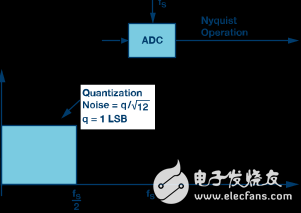
Figure 2a. Nyquist scheme. The sampling rate is FS and the Nyquist bandwidth is FS /2.
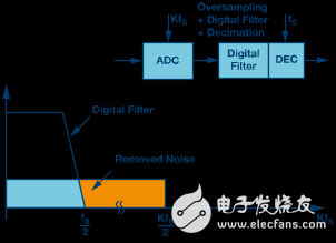
Figure 2b. Oversampling scheme. The sampling rate is K &TImes; FS.
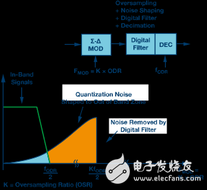
Figure 2c. Σ-Δ ADC scheme. Oversampling and noise shaping, sampling rate is FMOD = K &TImes; FODR.
One additional feature of the sigma-delta modulator is noise shaping, as shown in Figure 2c. The analog-to-digital conversion quantization noise is modulated and shaped, moving from low frequencies to higher frequencies (usually), and the low-pass digital filter removes it from the conversion result. The noise floor of a Σ-Δ ADC is determined by thermal noise and is not limited by quantization noise.
Sampling, modulation, filtering
The Σ-Δ ADC uses an internal or external sample clock. The ADC's main clock (MCLK) is often divided first and then used by the modulator; pay attention to this when reading the ADC data sheet and understand the modulator frequency. The clock transmitted to the modulator sets the sampling frequency FMOD. The modulator outputs data to the digital filter at this rate, and the digital filter (usually low pass with decimation) provides data at the output data rate (ODR). Figure 3 shows this process.
Force Sensor,Force Transducer,Strain Load Cell,Force Measurement Sensor
GALOCE (XI'AN) M&C TECHNOLOGY CO., LTD. , https://www.galoce-meas.com