Design of a Reusable High Speed ​​SPI Bus
For a long time, the mismatch between peripheral devices and host CPU speed has always plagued people, affecting the rapid development of computer systems and becoming the bottleneck of basic I/O systems. With the rapid growth of computer processing power and storage scale, this problem has become more prominent. To this end, people have adopted various software and hardware methods to continuously improve the interface performance between the CPU and I/O devices.
At present, embedded systems have been widely used in many fields such as communication and consumer electronics. However, in many applications, processor interface issues remain a bottleneck that constrains system performance. For a given design, there is little room for designers to face these cumbersome interface standards. They generally choose the appropriate standard product according to the cost and function required by the system, which may lead to interface standard conflicts and interoperability problems; perhaps the designer may re-select the standard device compatible with the interface, but may not meet the functional requirements Or system cost requirements, etc.
In the past few years, interface standards for eliminating data transmission bottlenecks between ICs, boards, and systems have emerged in an endless stream, providing a wide variety of interface technologies for communication system devices. Addressing interface and interoperability issues in digital system design is particularly important. The rapid development of FPGA technology has made the interface problem a good solution. For example, existing high-performance interface IP and high-speed physical I/O FPGA can meet the requirements of communication systems with data channels above 10Gb/s; FPGAs can be used to implement communication problems between interface-incompatible devices. Therefore, this paper will propose a new FPGA-based SPI interface design method.
SPI (Serial Peripheral Interface) serial peripheral interface bus [1] is a synchronous full-duplex serial communication interface bus. Because of its simple connection and convenient use, it is widely used. The SPI interface is used in many new devices such as LCD modules, FLASH, EEPROM memories, data input and output devices. However, in actual development applications, if the main controller does not have an SPI interface or needs to communicate with multiple peripherals with an SPI interface, the I/O of the main controller is used.
The port is simulated by software, which greatly limits the inconvenience of its application to data transmission. In an era of rapid development of FPGA technology, the most convenient way to solve this problem is to integrate an SPI core onto the chip.
Here, a reusable high-speed SPI bus is designed according to the industry standard SPI bus standard. Many variables in the design process are in the form of parameters. When applied in engineering practice, the parameters can be changed according to actual needs, which fully reflects the reusability.
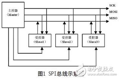
2 SPI bus principleThe SPI bus consists of four lines: the serial clock line (SCK), the master output slave input line (MOSI), the master input slave output line (MISO), and one slave select line (SS). The information is transmitted between the devices connected to the bus, and the connection manner is as shown in FIG. 1.
All data transfers in the SPI bus are synchronized by the serial clock SCK, which transfers 1 bit of data per clock pulse. SCK is generated by the master and is an input to the slave. The phase of the clock (CPHA) and polarity (CPOL) can be used to control the transmission of data. CPOL=“0†indicates that the SCK is at a low level, and CPOL = “1†indicates that the SCK is at a high level. Clock Phase (CPHA) can be used to select two different data transmission modes. If CPHA = '0', the data is valid on the first SCK edge after the signal SS is asserted. When CPHA = "1", the data is valid on the second SCK edge after the signal SS is asserted. Therefore, the clock phase and polarity of the SPI device in the master and slave must be the same to communicate.
The SPI can operate in either master mode or slave mode. In the master mode, each bit of data is transmitted/received with one clock action; in slave mode, each bit of data is transmitted/received after receiving the clock signal. A typical SPI system consists of a master MCU and one or several slave peripherals.
3 Design principlesThis system is described by the hardware description language verilog, which is a general structure that can be IP multiplexed.
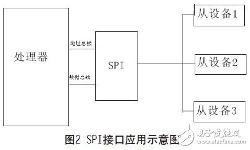
3.1 Typical applicationA typical application of the SPI interface is shown in Figure 2. The microprocessor and the slave implement bidirectional data transmission by sending instructions.
According to the principle of SPI bus, the SPI Master of this design is compatible with SPI protocol. The design on the host side is equivalent to the wishbone bus [2] specification compatible slave device. The overall architecture can be divided into the following three functional modules [3]: Clock generator The Serial interface and Wishbone interface are shown in Figure 3.
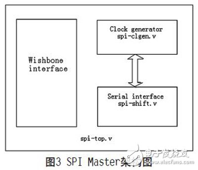
3.2.1 Clock Generation Module SPI-clgen Design
The source of the clock signal in the SPI clock divider module is the clock clk_in provided by the external system. The frequency of this clock is higher than the clock frequency used by the SPI bus. The module generates the corresponding clock output according to the clock division factor register of each interface. The signal clk_out acts as a serial clock. Since the SPI does not have a response mechanism, the timing requirements for transmission are quite strict. In order to ensure the reliability of the timing, a clock generation module which is abnormally reliable for odd or even frequency division is specially designed to generate transmission. Serial clock.
Shenzhen Xcool Vapor Technology Co.,Ltd , http://www.xcoolvapor.com