Design of non-synchronous buck regulator based on light load operation
Typically, the buck regulator is designed for continuous mode operation, which simplifies output voltage calculation and system design. However, if the system is asynchronous and requires operation under light load conditions, the situation becomes more complicated. Under these conditions, the buck regulator may instead operate in discontinuous mode. The duty cycle changes from the output voltage to the input voltage (Vout/Vin) to a complex function involving the inductor value, input voltage, switching frequency, and output current.
normal workFigure 1 shows the floating gate driver output driver section of the buck controller of the buck regulator when the system is powered up. The reference voltage, Vref, which is used to boost energy efficiency, powers the NFET gate driver until the diode voltage drops below the reference voltage, allowing the driver to fully operate. There is enough voltage to drive the gate (G) of the FET because the initial condition specifies that the output is 0V, so the source (S) voltage of the FET (Q1) is also 0V.
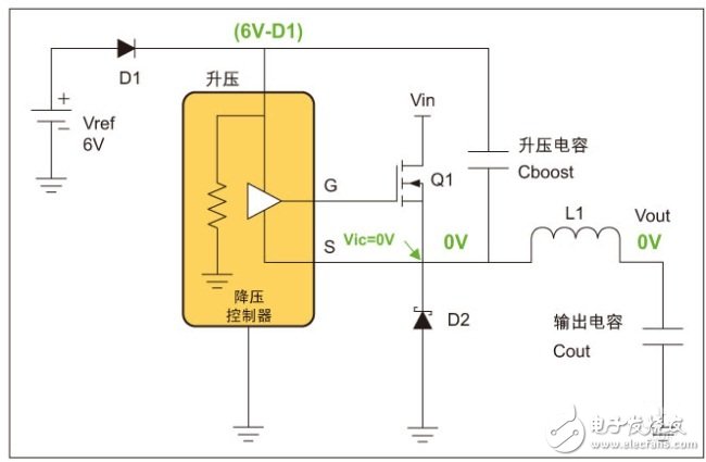
Figure 1. Buck regulator during power.
FlybackEnough load allows the system to work properly in continuous mode. During the flyback event caused by the FET being turned off (see Figure 2), there is always current flowing through the external FET or D2 to the inductor. The flyback event produces a voltage at the source of Q1 that is limited by the D2 voltage drop. There will be a negative voltage to ground. Similarly, because the boost capacitor (Cboost) switch raises the gate voltage, there is enough voltage to drive Q1; the boost capacitor supplies high voltage to the boost pin and provides the Q1 source (S). Corresponding negative voltage.
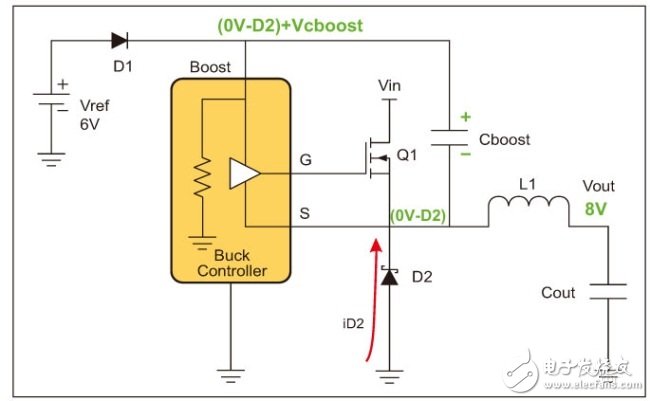
Figure 2, flyback conditions.
transitionDuring light load conditions where the average current demand is less than half of the current ripple, the system will enter a discontinuous mode. This is caused by the condition of the output current to be driven by the reverse regulation of the diode (D2). The output is likely to overshoot (because the control loop has a slower response time) and hangs at the overshoot position, and misses the pulse due to the lack of demand due to higher voltages, which is often a bit unpredictable.
problem lies inBut there are more issues to worry about in the circuit setup we are reviewing. After Q1 is turned off, the boost capacitor (Cboost) begins to discharge through the boost pin (Iboost), supplying current to any supporting circuit, and providing leakage current through D1, as shown in Figure 3. The extended turn-off time of Q1 in discontinuous mode begins to discharge the charge accumulated in the boost capacitor and drops it to a critical level if the charge is allowed to drop sufficiently. Once the critical level is exceeded, the Q1 FET will not turn on (may vary from component to component, but typically the boost capacitor voltage is approximately 3V). The source of the FET is approximately maintained at its regulated voltage (8V in Figure 3, depending on
Output load and output capacitor Cout value). Q1 is turned on after the output capacitor is fully discharged and the Q1 source is supplied with a voltage sufficiently low relative to the boost pin voltage (6V-D1) via D1.
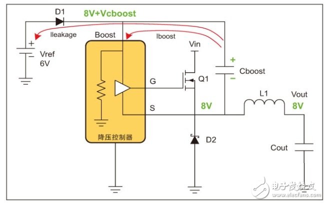
Figure 3. The boost capacitor discharges.
in conclusionDesigners should carefully evaluate the switching power supply design under all load conditions. Factors considered include over temperature. High temperatures will create an environment with a larger leakage current. The temperature coefficient of the current flowing into the boost pin is unknown, so the designer also needs to check for low temperature conditions. This result should also be used in the worst-case evaluation simulation process to complete the system evaluation and determine the minimum capacitance value. Careful design can also add engineering buffers to calculations.
The solutions that focus on the issues discussed in this article include:
1. Increase the boost capacitor (Cboost) value to eliminate low voltage discharge events.
2. Turn to the components of the gate driver that use the ground reference.
3. Modify the design to work in sync.
4. Change the reference voltage (voltage boost) connected to D1.
5. Replace D1 with a low leakage Schottky diode.
Trolley Speaker,Bluetooth Trolley Speaker,Portable Speaker Trolley,Trolly Speaker With Mic
GUANGZHOU SOWANGNY ELECTRONIC CO.,LTD , https://www.jerry-power.com