Introduction and design analysis of 3G multi-band transceiver
Most of the current 2G and 2.5G cellular networks operate in four frequency bands in the RF spectrum. Since these four frequency bands are globally planned, this means that if a user carries his mobile phone to other countries, the RF part of the mobile phone is likely to work in different frequency bands or frequencies. This requires a handset design that provides multiple configurations of parallel switches and key components such as power amplifiers (PAs) and surface acoustic wave (SAW) filters. But due to the maturity of the technology and the capacity of the 2G market, as well as advanced packet technology and integrated IC transceiver design, these parallel designs minimize the cost and volume of such handsets.
Figure 1 shows the design architecture of a typical quad-band GSM transceiver. Through integration, only three main components are required on the signal link: 1. Multi-band PA and integrated switch module; 2. Quad-band Rx SAW filter bank; 3. Silicon transceiver.
The 3G situation is somewhat similar to the previous cellular system in question. The spectrum initially allocated to the UMTS 3G system is the first frequency band. In this case, the required RF front-end is relatively simple, and an external filter can be used, which does not require much cost and PCB area overhead. However, due to different regions and regulatory restrictions, as well as the licensing of new spectrum, there are currently 10 bands allocated to 3G networks worldwide, but some of these bands overlap. Now users of 2G networks can think of continuing to use their mobile phones when traveling, so 3G users certainly expect this. This is especially important for high-end users, whether it's data or voice, because these users are usually business users and early adopters of 3G technology. Therefore, a more cost effective multi-band transceiver design is needed. Figure 2 shows the current band allocation map. A typical multi-band handset should now be able to cover all three bands, a low band and two high bands.
The easiest way to achieve the desired multi-band functionality is to use the current single-band transceiver design, which is to set up several front-end modules in parallel. The RF transceiver circuitry is very similar, except that the external matching and RF filters need to be specifically designed to fit the operating frequency band required by the handset. This approach is well achieved with careful frequency planning, wideband PLL systems, and high integration of sub-micron CMOS processes. However, considering the cost of the chip, the degree of integration, the number of external components, and the PCB area occupied by the RF transceiver, this solution is not an ideal solution. A practical example of this type of scheme is shown in Figure 3, except that the GSM part was removed for simplicity.
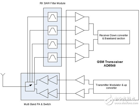
Figure 1: An example of a quad-band GSM transceiver that utilizes only three devices.
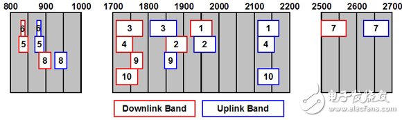
Figure 2: Frequency allocation diagram for the 3GPP band.
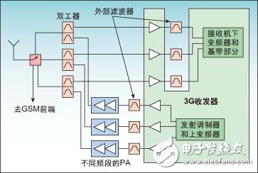
Figure 3: Example of a 3G multi-band transceiver front end implemented with a single-band design combination.
The Othello-3 family of 3G transceivers employs a bold processing architecture that removes the barriers associated with front-end integration. The biggest obstacle is the need for an external filter because the filter defines the input and output frequency ranges for a certain operating band. In a full-duplex system such as WCDMA, the transmitter and the receiver operate simultaneously, so a duplex filter is always required at the antenna to prevent high-power transmission signals from degrading the performance of the high-sensitivity receiver. However, due to circuit limitations, for front-end design, it is often necessary to design additional separate device filters on each of the transmit and receive channels, as shown in Figure 3.
Transmitter architectureA common superheterodyne transmitter architecture is shown in Figure 4.
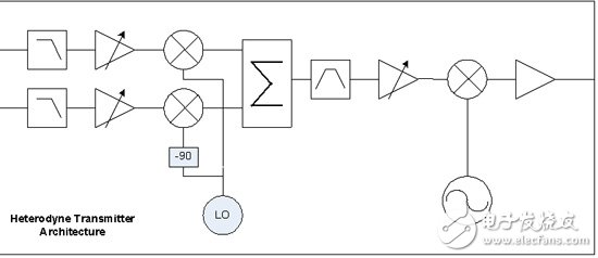
Figure 4: Superheterodyne transmitter architecture.
The filtered I/Q baseband input signal is mixed with an orthogonal local oscillator signal (LO) and then produces a constant intermediate frequency (IF) signal, which is typically located in the low to mid range of the megahertz stage. Since this is a mixed signal, it needs to be filtered to remove spurious signals, local oscillator signals and harmonic signals. The second output is then mixed with a variable frequency oscillator to form the RF output signal required for the final desired channel. Gain control is assigned in different parts. However, to filter out unwanted frequencies and ensure that the noise and harmonics required by the receiver band are met, an external SAW filter can greatly alleviate the design requirements of the integrated Tx channel. The filtered band-limited single-ended output signal is sent to the PA and duplexer, completing the front-end transmit chain.
The Othello-3 family of 3G transceivers uses a direct conversion or "zero heterodyne" transmitter architecture in which orthogonal baseband signals are directly upconverted to the RF carrier. This eliminates the need for secondary mixing and eliminates the associated RF parasitics and various unwanted frequency filter circuits, making it possible to remove external filters. However, since there is no Tx filter attenuation, other things need to be considered, mainly the noise level of the receiver band as described above.
To solve this problem, the Othello-3 family includes a special modulator core design that eliminates the noise source of the LO channel, which is traditionally far from the carrier (eg, receiver band). The main modulation noise at the frequency. Othello-3's 86dB gain control is also dismembered into the modulator core, eliminating the need for additional circuitry on the signal path, reducing the associated noise contribution. Low-noise design techniques run through the entire transmitter design, eliminating the need for additional filtering to meet out-of-band noise requirements. This ensures the best performance under all operating conditions. Calibration is all self-calibrating without user input. The modulator circuit is generally the same as all IC designs, with fully differential signal processing. However, the Othello-3 also comes with a balun with a single-ended output impedance of 50 ohms that can be sent directly to the PA module without external Match the original.
The Othello-3 transmit channel also provides excellent error vector magnitude (EVM) and adjacent channel leakage ratio (ACLR) performance. Eliminating the external SAW filter on the transmit channel greatly reduces material cost and PCB area and paves the way for multi-band PA integration. As seen in the GSM market, all four bands can be included in a single PA package. .
Direct conversion receiverThe direct conversion receiver architecture used on all Othello transceivers is an excellent and proven transceiver architecture due to its high level of integration. In a GSM receiver, the entire receive signal chain can be integrated. For 3G systems where transmitter signal leakage to the receiver is a problem, an interstage filter was previously required, as shown in Figure 3. This reduces the previous transmit signal leakage of the critical mixing stage. Setting a SAW filter after the low noise amplifier (LNA) ensures that the filter loss does not affect the receiver sensitivity, but it is an obstacle to integration.
Othello-3 consists of three LNA modules, two for the high band and one for the low band. Each LNA has a single-ended input that can be easily matched to its own duplex filter. Each LNA includes an optimum bandpass response to reduce the level of the out-of-band signal and the leakage of the transmitter signal to the mixing stage. Othello-3 also features a high linearity mixer design that eliminates the need for an external interstage filter, as shown in Figure 5. Receiver gain control is optimally distributed to the RF signal chain and baseband processing stages. To facilitate gain programming and calibration, Othello-3 includes integrated gain distribution logic. The baseband only needs to write a single gain word into the chip to automatically achieve optimal gain distribution under maximum dynamic range conditions.
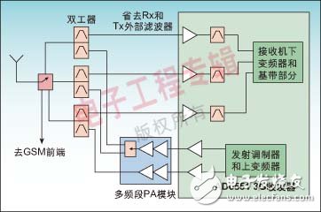
Figure 5: The AD6551 front-end architecture with the external filter removed.
The example above illustrates the integration of 3G RF devices, and the vendor is also experimenting with antenna switch modules that include all front-end modes and integrated band switches with GSM Rx SAW filter banks.
The ADI Othello-3 transceiver is currently comprised of the AD6551, which is best suited for WCDMA 3G handsets, while the AD6552 is suitable for 3G TD-SCDMA mode. Both devices are available for 3GPP Release 5 and HSDPA mode of operation.
Summary of this articleThe current single-mode 2G handsets can implement the entire quad-band RF solution using only three major chip packages. This solution has minimal space and has the required design features. The initial 3G handsets were limited to single-band mode and relied on external filters to meet the metrics, but this architecture is not the best choice for multi-band handset designs, both in size and cost. Othello-3 eliminates the need for external filters, enabling further integration of front-end devices and PAs in current 3G transceiver designs. With advances in integration technology and switch design, more and more front-end devices can be integrated step by step, but with a transceiver such as Othello-3, a fully optimized multi-mode architecture can be realized.
Low Frequency Inverter Charger
Low Frequency Inverter Charger
Have good environmental adaptability. Resistant to high temperatures, dust, stable output. Suitable for outdoor, vehicle, office space.
Low Frequency Inverter Charger,Low Frequency Inverter 24V,Low Frequency Inverter,Car Power Charger
SUZHOU DEVELPOWER ENERGY EQUIPMENT CO.,LTD , https://www.fisoph-power.com