Military UAVs in China _ Domestic Military UAV Rankings
Military drones are unmanned aircraft that are controlled by remote control equipment or by self-contained procedures. According to its control method, it is mainly divided into three types: radio remote control, automatic program control and integrated control. With the wide application of high and new technology in weapons and equipment, the development of drones has made breakthrough progress, and has appeared frequently in several local wars. It has repeatedly won meritorious deeds and has been highly praised by military personnel from various countries. It can be predicted that in the 21st century battlefield, people will face an increasing number of drones, and military drones will reshape the 21st century combat mode.

As one of the modern air military forces, the military drone has the characteristics of no casualties, limited use restrictions, good concealment and high efficiency. The status and role in modern warfare are increasingly prominent in recent local wars. .
The military drone has the characteristics of exquisite structure, strong concealment, convenient use, low cost and flexible maneuverability. It is mainly used for battlefield reconnaissance, electronic interference, carrying cluster bombs, guided missiles and other weapons to perform offensive tasks, and as an airborne Communication relay platform, nuclear test sampler, nuclear explosion and nuclear radiation reconnaissance aircraft.

Intelligence reconnaissance
The reconnaissance drone can realize all-weather comprehensive reconnaissance capability by installing various sensors such as photoelectric and radar. The reconnaissance method is efficient and diverse, and can perform high-speed information scanning over the battlefield. It can also fly at low speed or hover gaze to provide real-time intelligence support for the troops. . The drone can penetrate deep into the enemy's hinterland and try to be close to the enemy signal radiation source, which can intercept important low-power close-range communication signals on the battlefield, and the advantage is particularly obvious. The high-altitude long-time strategic reconnaissance drone passes over the reconnaissance target, replacing some of the functions of the satellite, and performing high-altitude reconnaissance missions with high-resolution camera equipment to capture clear ground pictures is of strategic importance. The portable drone meets tactical tasks such as troop-level battlefield surveillance, target reconnaissance, and damage assessment. In the Iraq war, US military drones provided 50% of reconnaissance intelligence about enemy fixed and moving targets. The entire process of distributing and delivering intelligence does not exceed 10 minutes.
2. Military strike
The drone can carry a variety of precision attack weapons, attack the ground and sea targets, or carry air-to-air missiles for air combat, and can also carry out anti-missile interception. The combat drones carry combat units and discover important targets for real-time attacks to achieve “inspection and combinationâ€. It can reduce casualties and increase the ability of troops to attack. The combat drone can be deployed in advance to intercept the tactical missiles in the booster segment, destroying the incoming missiles at a longer distance as the air defense. The attack-type anti-radiation drone carries small and powerful precision guided weapons, laser weapons or anti-radiation missiles, and attacks on radar and communication command equipment; tactical attack drones can replace missiles in some combat areas. Take a suicide attack to carry out a one-time attack on the enemy; the main battle attack drone is large, fast, ground attack and air combat, attacking and intercepting ground and air targets, is an important means to achieve global rapid strike capability. In the NATO air strike against Libya, the "predator" was used to launch the "Halfa" missile to carry out air strikes against Libya, to accurately strike ground targets, and also to fight the Mi-25 fighter. Be the first military drone to directly engage in air combat.
3. Information confrontation
Due to its unique advantages, the UAV can take off at any time in the harsh environment on the battlefield, and conduct countermeasures against photoelectric information such as laser guidance, microwave communication, command network, and complex electromagnetic environment, effectively blocking the attack, command and enemy equipment. Reconnaissance ability to improve the efficiency of information on their own. The electronic countermeasure drone performs reconnaissance and interference on the command communication system, ground radar and various electronic devices, and supports various attack aircraft and bomber operations: the decoy drone carries a radar echo enhancer or an infrared simulator to simulate an air target. Deceive enemy radars and missiles, induce enemy radar and other electronic reconnaissance equipment to start up, lure enemy air defense weapons to shoot, and cover up their own aircraft to stand out; UAVs can also carry out psychological warfare by throwing propaganda materials and calling on enemy battlefields. .
4. Communication relay
In the future war. The communication system is the lifeline of battlefield command and control, and it is the focus of attacks by both sides. The UAV communication network can establish a powerful redundant backup communication link to improve survivability. After being attacked, the backup communication network can be quickly recovered, playing an irreplaceable role in the network center battle. The high-altitude long-endurance drone expands the communication distance, uses satellites to provide alternative links, and directly links with land-based terminals to reduce the threat of physical attacks and noise interference. The combat communication drone adopts a variety of digital transmission systems, and the line-of-sight analog data transmission system is adopted between each combat unit. An over-the-horizon communication relay system is used with the satellite to transmit images, data and other information in real time at high speed.
5. Logistics support
With the development of drone technology. Its mission area is also constantly expanding. In recent years, the US military has begun to explore the use of drones to carry out logistical support tasks such as material transportation, fuel replenishment, and even the evacuation of the wounded and sick. When the drone is under such a task, it has the advantages of being unaffected by the complicated terrain environment, fast, and avoiding the ambush of the ground enemy. It also has the characteristics of low cost, easy operation and so on. The K-MAX unmanned helicopter developed by American Karman Airlines successfully completed the world's first unmanned aerial cargo mission in Afghanistan on December 17, 2011. It has been deployed for a long time in the battlefield in Afghanistan.

The "Pterosaur" UAV has a fully autonomous platform, portable equipment and small open space combat weapons, as well as various reconnaissance surveillance and ground attack missions, which can be used for stability, counter-terrorism, border patrols, etc. In addition, it can be widely used in civil and scientific research. With the ability to guarantee attendance, it conducts high-intensity continuous operations and launches thousands of weapons. In addition, the "Pterosaur" drone can withstand the test of a variety of cruel conditions, desert high temperature, cold and windy, mountainous terrain, marine environment, etc., are not to mention. Many times of anti-terrorism operations, border control, intelligence gathering and other tasks have also achieved satisfactory results. It can be seen that its adaptability and combat capability are very strong.

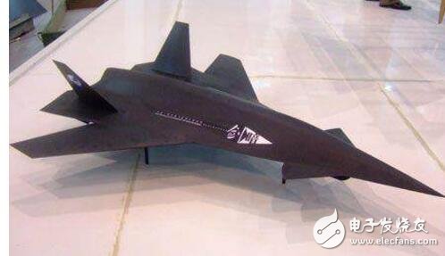
The "Dark Sword" uses an arrow-shaped wing-body fusion layout similar to the B-2 and F-117 hybrids in the aerodynamic design. The fuselage section presents an arrow-shaped triangle in the vertical direction, a flat streamlined fuselage and wings. The sleek transition into an overall lifting surface, the body design can be combined with the retractable front wing, conventional wing and tail to form an overall layout suitable for high speed and large overload maneuvering. It is speculated from the appearance that the "dark sword" should have supersonic speed, high maneuverability and stealth performance, and has reached the high level of international fighter technology.
What is Multilayer PCB
Definition of Multilayer PCB Circuit Board
The multilayer PCB came into being due to the evolving changes in the electronics industry. The functions of electronics have become progressively more sophisticated over time, requiring more complex PCBs. Unfortunately, PCBs were limited by problems like noise, stray capacitance and crosstalk, and therefore needed to follow certain design constraints. These design considerations made it difficult to get a satisfactory level of performance from a single or even double-sided PCB - thus the multilayer PCB was born.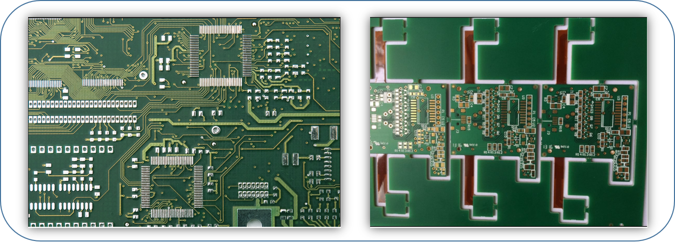
Why Do We Need Multilayer Circuit Boards?
Multilayer PCB is an integral part of most of the electronics when it comes to connecting number of electronic components on the board. Multilayer PCB helps us getting rid of the old ways of joining components where components were joined together by end to end wiring, resulted in covering more space and weight and unable to fulfill the requirements of more complex designs. Experts are in constant struggle to improve electronic design with compact shape so it provides better user experience and turns out to be less costly than its predecessors.Now, you have got a clear idea why do we need PCB. There are already different types of PCB board available in the market i.e. single layer board and double layer board. But, sometimes these boards fail to deliver more complex designs because of availability of less number of conductive layers on the board. Technology is evolving with the greater need of making devices cheap and low weight so they can meet the requirements in less cost and capable of performing more functions than using conventional ways of making electronic devices.
Multilayer Circuit Board Can Simplify The Design
Multilayer PCB boards came into play with the intention of constructing more number of conductive layers on the board than single-layer or double-layer boards. Multi-layer boards come with a combination of single-layer or double-layer board and give opportunity to connect more electronic components in less space. These boards are made with number of conductive layers with insulated material between them. Multilayer boards are mostly developed in rigid form, because making multilayer board in flexible form is very difficult to achieve and it also results in more cost than rigid boards. Instead of using flexible multilayer boards, most of the professionals prefer using combinations of single or double sided board that are very effective in most of cases and are cheaper than multilayer flexible boards.Development of multilayer PCB board totally depends on customers'demands. With the invention of new technology multilayer circuit boards can be manufactured with up to 100 conductive layers, making complex design where more number of components are joined together. Smartphones are a great example of multilayer PCB that gives a benefit of performing more functions using single board. This refrains from spending more money on the combination of single sided or double sided boards, because they cost heavily with no guarantee of fulfilling requirements as multilayer PCB.
Multilayer PCB Board Fabrication
Multilayer boards can be manufactured with even conductive layers or odd conductive layers on them. However, it is recommended to use multilayer PCB with even layers because it results in simple design and helps in joining number of different components on the board where board design with odd layers can be costly and pertains to complex design, making it difficult to join number of electronic components on the board. Also, design with odd layers makes it very difficult twisting the board during execution of project, as odd layers are not equally distributed over the whole board structure which can damage the boards when they are subject to under heavy weights.Some multilayer boards are manufactured so closely, making it very difficult of you to count the total number of layers with naked eye. However, still you can guess total number of layers based on the layers pattern and how they are laminated on the board. Number of different conductive layers on the multilayer boards can be termed as signal, power or ground planes. Power or ground planes are directly proportional to the number of voltage requirements on the board, if there is a need of more than voltage supply on the board, then multilayer boards come with more than one power or ground planes.
The difference between single-layer PCB, Single Sided PCB, and multi-layer PCB
Single layer PCB vs multilayer PCB
When it comes to printed circuit boards, an immediate question before design is whether to use single or multi layered PCBs for your circuit. The benefit and use of each depends entirely on what you`re intending to do. First we should define each type of circuit board.
Single layer or single sided PCB
These PCBs simply have components on one side of the board and the conductor pattern on the other side. This reason is why it`s known as a single sided or single layer PCB. Often, these are used for simpler devices as no wires can cross if the circuit is to function correctly. These are usually slightly cheaper to manufacture than multi layer PCBs.
How to identify a multilayer PCB
If you have some PCBs to hand and you`re interested in how many layers it uses, there is a way to see without causing damage to the board itself.
Firstly, shine a light into the edge in an attempt to see the copper planes, this may result in you seeing the signal traces. This will only work if the copper comes close to the edge however.
Using some sort of bright light source again, we can see if a board has inner layers even if doesn`t have blind vias. The best place to do this is [where there aren`t traces/planes on the visible, outer layers-" The areas where it`s blocked are usually copper.
Some companies or manufacturers are known to label the individual layers on the board itself, so check around the edges for numbers.
How Are Multilayer PCBs Fabrication?
Packing the power of a double-layer PCB into a format that's a fraction of the size, multilayer PCBs are becoming increasingly popular in electronics. They come in a wide range of sizes and thicknesses to accommodate the needs of their expanding applications, with variants ranging anywhere from four to twelve layers. Layers most often come in even numbers, since odd numbers of layers can cause issues in the circuit like warping, and are no more cost-effective to produce. Most applications require between four and eight layers, though applications like mobile devices and smartphones tend to use around twelve layers, and some professional PCB manufacturers boast the ability to produce multilayer PCBs with nearly 100 layers. Multilayer PCBs with that many layers are rare to see, however, as they are extremely cost-inefficient.
-
multilayer PCB stackup

4 Layer PCB Stack up
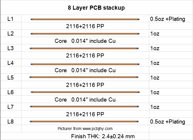
8 Layer PCB stackup
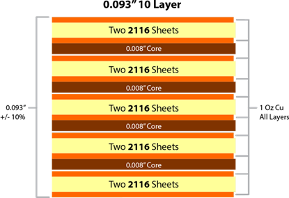
10 Layer PCB Stack UP
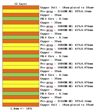
12 Layer PCB Stack UP
-
Specialized equipment for pressing multilayer
PCBs Manufacturing multilayer PCBs requires a specialized hydraulic press with heated platens. Initially the books are squeezed with a [kiss" pressure of 50 psi prior to being heated to 350F at 350 psi for a minimum of one hour. The assembly is then allowed to cool slowly before removal for further processing. At Omni, the maximum size of a multilayer board is 12"x 16" while the board thickness can range from 0.015"to 0.125".
-
Multilayer PCBs Fabrication Process
The outer layers of multi-layer consist of sheets of glass cloth pre-impregnated with uncured epoxy resin (prepreg) and a thin copper foil.
The lay-up operator has already placed a copper foil and 2 sheets of prepreg on the heavy steel baseplate. Now he places the pre-treated core carefully over the alignment pins. Then he adds 2 more sheets of prepreg, another copper foil and an aluminium press plate
He builds up 3 panels on the baseplate in the same way. Then he rolls the heavy stack under a press which lowers down the steel top plate. He pins the stack together and rolls the finished stack out of the clean room into a rack.
The press operator collects 3 stacks on a loader and loads them into the bonding press. This press uses heated press plates and pressure to bond the layers of the PCB together. The heat melts and cures the epoxy resin in the prepreg while the pressure bonds the PCB together. The process is computer controlled to build up the heat and the pressure correctly, hold it and then to cool the press down. In this way we ensure a permanent bond that will last the lifetime of the PCB. Our board has 4 layers but complex PCBs for defence, avionic and telecommunications applications can have more than 50. These may include sub-assemblies of cores, prepregs and foils drilled and plated before being assembled into the final PCB.
Once the cycle is completed the press operator unloads the press and carefully rolls the heavy stacks into the clean room. Here the lay-up operator de-pins the stack and removes the top plate. He unloads each of the panels from the stack, removing the aluminium press plates used to ensure a smooth copper finish. The copper foil is now bonded in place to form the outer layers of the PCB.
Design for Manufacturability (DFM) for multilayer circuit boards
PCB design plays an important role in determining the mechanical,electrical and thermal performance of the complete electronic system. Many advanced electronic components use multilayer PCB, because it allows large number of components to incorporate on a single board, hence allowing the higher component density. Some PCBs are highly complex that make use of electronic components that are embedded on the substrate material.
Signal integrity and power integrity are two important features you must take into consideration before you intend to make PCB layout design. You must adopt following rules in order to maintain complete power integrity and signal integrity of the PCB.

- Conductive PCB trances are composed of copper that comes with finite resistance. Voltage drop in many digital systems can severely influence the quality and accuracy of the system at that resistance when small current flows through the system. Controlled impedance trances are required in order to maintain the high accuracy of the system.
- If significant current flows through the board, it exceeds the temperature beyond normal value because of the resistance of trances.In order to control board temperature and increase PCB reliability, the width of the trances must be increased, which, if not possible due to the overall predefined circuitry, then copper thickness must be increased to 2 to 3 based on your needs and requirements.
- Stray inductance can cause voltage spikes on the board which can be handled by using the decoupling capacitors near load.
- Magnetic field is generated when current passes through the traces. This magnetic field can harm or influence the compoents that come under the range of magnetic field. To avoid this process, components must placed with larger space between them which is near to impossible in case of multilayer compact design. So, alternative way to overcome the affect of magnetic filed is to add return path or ground plane. A ground plane will behave like a shield and helps in providing a return path of any signal. Ground planes generates decoupling in multilayer PCBs.
- Analog and digital portions of the circuit must be separated from the ground planes and they must be connected at a single point
- It is recommended to avoid 90 degree trances because of EMI issues.
- Better to avoid long tracks for the traces containing both analog and digital signals. Noise coupling can be avoided if both signals cross at one point.
Bow and Twist in multilayer PCBs is typically the result of unconventional designs.
Bow and twist is more likely to occur in asymmetric designs which can result in unbalanced stress conditions. For example, odd layer counts (3, 5 layer) are known to cause issues. Another source of multilayer PCB bow and twist comes from designs which specify variable layer thicknesses. For example, a 4 layer build specification of 7 / 28 / 21 creates more risk of deformation than a standard build. Even different circuit configurations can be influencing factors.
Multilayer PCB Thickness Parameters
| Standard Multilayer Builds | Mils per Dielectric Layer | Resulting Thickness |
| 4 Layer | 14 / 28 / 14 | 62 mil |
| 6 Layer | 7 / 14 / 14 / 14 / 7 | 62 mil |
| 8 Layer | 7 / 5 / 11 / 5 / 11 / 5 / 7 | 62 mil |
| 10 Layer | 4 / 5 / 7 / 5 / 7 / 5 / 7 / 5 / 4 | 62 mil |
So how can understanding more about the PCB multilayer assembly process help you reduce your PCB costs?
Ensure the specifications you are requesting are truly needed. While deviations from standard [tried and true" recipes are often possible, each subtle change carries additional risk, usually reflected in higher pricing, slower delivery times and occasional failure which could require a re-design. Additionally, we strongly recommend electrical testing for most multilayer printed circuit boards. Today`s software has helped designers provide consistently more manufacturable PCBs and you should expect even better results when you infuse your designs with the considerations provided above.
Multilayer PCB Disadvantages
The benefits of multilayer PCBs are numerous, making them applicable to a wide variety of advanced technologies. However, these types of PCBs aren't appropriate for all applications. In fact, several drawbacks can outweigh multilayer PCB advantages, especially for electronics of lower cost and complexity. These disadvantages include the following:
- Higher Cost: Multilayer PCBs are significantly more expensive than single and double layer PCBs at every stage of the manufacturing process. They are difficult to design, taking an extensive amount of time to work out any potential problems. They also require a highly complex manufacturing process to produce, which takes a great deal of time and labor on the part of assembly personnel. Additionally, due to the nature of these PCBs, any mistake in the manufacturing or assembly process is prohibitively difficult to rework, resulting in either additional labor costs or scrap material expenses. On top of it all, the equipment used to produce multilayer PCBs is quite expensive because it is still a relatively new technology. For all those reasons, unless small size is an absolute necessity for the application, cheaper alternatives may be a better choice overall.
- Complicated Production: Multilayer PCBs are more difficult to produce, requiring much more design time and careful manufacturing techniques than other PCB types. This is because even small flaws in the PCB's design or manufacture could render it useless.
- Limited Availability: One of the largest issues with multilayer PCBs is the expenses of the machinery needed to produce them. Not all PCB manufacturers have the funds or the necessity for this machinery, so not all PCB manufacturers carry it. This limits the number of PCB manufacturers available to produce multilayer PCBs for clients. Thus, it's best to carefully inquire a PCB manufacturer's capability in terms of multilayer PCBs prior to deciding it as your contract manufacturer.
- Skilled Designer Required: As previously discussed, multilayer PCBs require extensive design beforehand. Without previous experience, this can be problematic. Multilayer boards require interconnection between layers, but must simultaneously mitigate crosstalk and impedance issues. A single problem in the design can result in a non-functioning board.
- Production Time: With increased complexity comes more manufacturing requirements. This plays into a key issue with multilayer PCBs' turnover rate – each board requires a significant amount of time to produce, resulting in more labor costs. Additionally, it possibly leads to longer periods between when an order is placed and when the product is received, which can be a problem in some circumstances.
However, these issues do not diminish from the utility of multilayer PCBs. While they tend to cost more than a single layer PCB, a multilayer PCB claims many advantages over this type of printed circuit board.
Multilayer PCB Benefits
From a technical point of view, multilayer PCBs present several advantages in design. These benefits multilayer PCBs present include:
- Small Size: One of the most prominent and lauded benefits of using multilayer PCBs lies in their size. Because of their layered design, multilayer PCBs are inherently smaller than other PCBs with similar functionality. This presents a major benefit to modern electronics, as the current trend is working toward smaller, more compact yet more powerful gadgets like smartphones, laptops, tablets and wearables.
- Lightweight Construction: With smaller PCBs comes less weight, especially as the multiple connectors required to interlink separate single and double-layered PCBs are eliminated in favor of a multilayered design. This, again, is beneficial for modern electronics, which are geared more toward mobility.
- High-Quality: Due to the amount of work and planning that must go into the creation of multilayer PCBs, these types of PCBs tend to be better in quality than single and double-layer PCBs. They also tend to be more reliable as a result.
- Increased Durability: Multilayer PCBs tend to be durable by their nature. Not only do these multilayer PCBs have to withstand their own weight, but they must also be able to handle the heat and pressure used to bind them together. On top of these factors, multilayer PCBs use multiple layers of insulation between circuit layers, binding it all together with prepreg bonding agent and protective materials.
- Enhanced Flexibility: Though this does not apply to all multilayer PCB assemblies, some do use flexible construction techniques, resulting in a flexible multilayer PCB. This can be a highly desirable trait for applications where mild bending and flexing may occur on a semi-regular basis. Again, this does not apply to all multilayer PCBs, and the more layers incorporated into a Flexible PCB , the less flexible the PCB becomes.
- More Powerful: Multilayer PCBs are extremely high-density assemblies, incorporating multiple layers into a single PCB. These close-quarters enable boards to be more connective, and their innate electrical properties allow them to achieve greater capacity and speed despite their smaller size.
- Single Connection Point: Multilayer PCBs are designed to work as a singular unit, rather than in tandem with other PCB components. As a result, they have a single connection point, rather than the multiple connection points required to use multiple single layer PCBs. This proves to be a benefit in electronic product design as well since they only need to include a single connection point in the final product. This is particularly beneficial for small electronics and gadgets designed to minimize size and weight.
These benefits make multilayer PCBs highly useful in a variety of applications, particularly mobile devices and high-functioning electronics. In turn, with so many industries turning to mobile solutions, multilayer PCBs are finding a place in an increasing number of industry-specific applications.
Advantages of Multilayer PCBs over Single Layer Alternatives
- Higher Assembly Density: While single layer PCBs' density is limited by their surface area, multilayer PCBs multiply their density through layering. This increased density allows greater functionality, improving capacity and speed despite the smaller PCB size.
- Smaller Size: Overall, multilayer PCBs are smaller in size than single layer PCBs. While single layer PCBs must increase the surface area of the circuit by increasing size, multilayer PCBs increase surface area through the addition of layers, decreasing overall size. This allows for higher-capacity multilayer PCBs to be used in smaller devices, while high-capacity single layer PCBs must be installed into larger products.
- Lighter Weight: The integration of components in a multilayer PCB means less of a need for connectors and other components, resulting in a lightweight solution for complex electrical applications. Multilayer PCBs can accomplish the same amount of work as multiple single-layer PCBs, but does so at a smaller size and with fewer connecting components, reducing weight. This is an essential consideration for smaller electronics where weight is a concern.
- Enhanced Design Functionality: Overall, multilayer PCBs are capable of being more than the average single layer PCB. With more incorporation of controlled impedance features, greater EMI shielding and overall improved design quality, multilayer PCBs can accomplish more despite their smaller size and lesser weight.
So, what do these factors mean when deciding between a multilayer and single layer construction? Essentially, if you're looking to produce a small, lightweight and complex device where quality is essential, a multilayer PCB is likely your best choice. However, if size and weight are not primary factors in your product design, then a single or double layer PCB design may be more cost-effective.
Multilayer PCB Applications
The advantages and comparisons discussed above beg the question: what's the use of multilayer PCBs in real world? The answer is just about any use.
For numerous industries, multilayer PCBs have become the preferred option for a variety of applications. Much of this preference derives from the continuous push across all technology toward mobility and functionality. Multilayer PCBs are the logical step in this progression, achieving greater functionality while reducing size. As such, they've become fairly ubiquitous, used in many technologies including:
- Consumer Electronics: Consumer electronics is a broad term used to cover a wide range of products used by the general public. This tends to include products used on a daily basis, such as smartphones and microwaves. Each of these consumer electronics contains a PCB, but an increasing proportion of them are using multilayer PCBs instead of standard single layers. Why? Most of the reason lies in consumer trends. People in the modern world tend to prefer multi-function gadgets and smart devices that integrate with the rest of their lives. From universal remotes to smartwatches, these types of devices are fairly common in the modern world. They also tend to use multilayer PCBs for their increased functionality and smaller size.
- Computer Electronics: Everything from servers to motherboards uses multilayer PCBs, primarily for their space-saving attributes and high functionality. With these applications, performance is one of the most essential characteristics of a PCB, whereas cost is relatively low on the list of priorities. As such, multilayer PCBs are an ideal solution for many technologies in this industry.
- Telecommunications: Telecommunication devices often use multilayer PCBs in numerous general applications, such as signal transmission, GPS and satellite applications. The reason for this lies primarily in their durability and functionality. PCBs for telecommunications applications are often either used in mobile devices or towers outdoors. In such applications, durability is essential while still maintaining a high level of functionality.
- Industrial: Multilayer PCBs do prove more durable than several other options currently on the market, making them a good choice for applications where rough handling may be a daily occurrence. As such, multilayer PCBs have become popular in several industrial applications, most notable of which are industrial controls. From industrial computers to control systems, multilayer PCBs are used throughout manufacturing and industrial applications to run machinery, favored for their durability as well as their small size and functionality.
- Medical Devices: Electronics is becoming an increasingly essential part of the healthcare industry, functioning in every corner of the industry from treatment to diagnosis. Multilayer PCBs are particularly favored in Medical industry for their small size, lightweight nature and impressive functionality compared to single-layer alternatives. These benefits have led to multilayer PCBs being used in modern X-ray equipment, heart monitors, CAT scan equipment and medical testing devices etc.
- Military and Defense: Favored for their durability, functionality and low weight, multilayer PCBs are useful in high-speed circuits, which is becoming an increasing priority for military applications. They're also favored due to the defense industry's increased movement toward highly compact engineering designs, as the small size of multilayer PCBs leaves more room for other components to flourish existing functions.
- Automotive: Cars are relying on electronic components more and more in the modern era, especially with the rise of electric cars. With everything from GPS's and onboard computers to headlight switches and engine sensors controlled by electronics, using the right kinds of components becomes increasingly essential in automotive design. This's why many auto manufacturers start to favor multilayer PCBs over other alternatives. While they are small and durable, multilayer PCBs are also highly functional and relatively heat-resistant, making them a good fit for the internal environment of an automobile.
- Aerospace: Like cars, jets and rockets rely heavily on electronics in the modern era, all of which must be extremely precise. From the computers used on the ground to those used in the cockpit, aerospace PCB applications must be reliable, able to handle the stresses of atmospheric journeys while simultaneously making enough room for the rest of the surrounding equipment. Multilayer PCBs present an ideal solution in this case, with plenty of protective layers to keep heat and outside stress from damaging the connections, as well as the ability to be made from flexible materials. Their higher quality and functionality also contributes to this utility in the aerospace industry, as aerospace companies prefer to use the best materials possible to keep their personnel and equipment safe.
- And Many More! Multilayer PCBs are used in a wide variety of other industries, including the science and research industry and even home appliances and security. Everything from alarm systems and fiber optic sensors to atomic accelerators and weather analysis equipment uses multilayer PCBs, taking advantage of the space and weight savings offered by this PCB format, as well as their heightened functionality.
Why Are Multilayer PCBs So Widely Used?
The specific applications listed above represent only a fraction of multilayer PCBs applied throughout the industry. But why are they used so widely?
Much of the favoritism toward multilayer PCBs lies in industry trends. With electronics progressing ever toward miniaturization yet multi-functional options, the internal components of those electronics must follow the same trend. While single and double-sided PCBs have proven limited in their ability to balance size and functionality, multilayer PCBs provide a comprehensive solution.
While there are several drawbacks to using multilayer PCBs over single and double-layer options, such as increased costs, design times and production inputs, these costs are becoming more accepted in today's world. Functionality is largely favored over cost, and people are willing to pay more for high capacity electronics. Additionally, as the technology becomes increasingly mainstream, production techniques and machinery will eventually become less expensive, especially as new techniques arrive in the industry.
With those irreversible trends and continuing progress of technology, many expect to see multilayer PCBs become even more abundant in the future.
Click on the following link to learn more about our products and services:
Multilayer PCB, PCB Board, Multilayer PCB Board, PCB Manufacturing
JingHongYi PCB (HK) Co., Limited , https://www.pcbjhy.com