Ultra-high speed ADC data reception design based on LVDS
Abstract: Ultra-high-speed ADCs usually use LVDS level to transmit data. The high sampling rate makes the output data rate very high, reaching the order of hundreds of megahertz to gigahertz. How to correctly receive high-speed LVDS data becomes a difficult point. In this paper, the data reception of ADS42LB69 chip is taken as an example. From the aspects of signal transmission and data decoding, the problems that should be paid attention to when implementing LVDS data reception and the specific implementation methods are detailed, and the correctness of the method is verified by experiments.

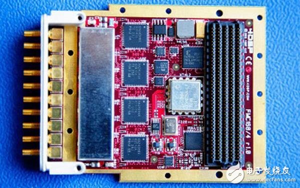
1 Introduction The software radio concept requires that the digitization of the radar system be as close as possible to the antenna, so the digital receiving system places high demands on the speed of the analog-to-digital converter. High-speed, high-precision ADCs output multi-bit high-speed data streams. The current mainstream data transmission level is low-voltage differential signaling (LVDS). The differential transmission characteristics of LVDS make it produce small electromagnetic interference, and can effectively suppress common mode noise and increase anti-interference ability. As the data rate increases, the time window for multi-bit data synchronization reception becomes smaller. How to ensure the correct reception of multi-channel data becomes a design difficulty. In order to reduce this difficulty, ADC devices are generally used in serial mode to complete the transmission of multi-bit sampled data with fewer data lines. In this paper, the method of realizing the correct reception of LVDS data is studied for the problem of multi-bit high-speed LVDS data transmission. ADS42LB69 is taken as an example to design a data acquisition board based on Xilinx FPGA platform. In the following two aspects of signal transmission and data decoding, the problems that need to be paid attention to in the design and the specific implementation methods are introduced in detail.
2 Signal transmission To complete the correct reception of data, first ensure the integrity of signal transmission, reduce distortion, and enable the receiving end to correctly obtain serial LVDS data. Signal integrity can be divided into timing, noise and electromagnetic interference. For high speed digital signal transmission, signal integrity includes both waveform integrity and timing integrity.
2.1 Waveform Integrity Waveform integrity refers to the influence of the transmission line on the electrical performance of the signal such as voltage, current and power. There are three main types of noise sources that affect waveform integrity: signal integrity of a single network, crosstalk between two or more networks, electromagnetic interference and radiation from the system. For each type of noise source, the design needs to be solved in different ways.
The first type of problem refers to reflections and distortion caused by discontinuities in impedance on the signal transmission path. Equation (1) gives the relationship between the reflection coefficient of the RF transmission line and the impedance of the transmission line (where γ is the reflection coefficient, which is the load impedance, and ZL is the characteristic impedance of the transmission line). It can be seen from the formula that when the load impedance is equal to the characteristic impedance of the transmission line, the reflection coefficient is zero, and the signal can be transmitted without distortion. Therefore, in order to ensure signal waveform integrity, the transmission line impedance is required to be continuous, and the impedance of the receiving end must be accurately matched. Transmission line impedance continuously requires special design when PCB layout, including 100Ω impedance control of differential signal lines, data lines should be routed in the same layer as possible, and the reference plane should be continuous. Load impedance matching is achieved by placing a 100 Ω resistor at the receiving end. In order to reduce the difficulty of layout, Xilinx FPGA integrates matching resistors inside, and the resistance can be configured according to application requirements.
When there is mutual inductance or mutual capacitance between the signal transmission path and the adjacent network, the signal will reach the other network from one network, causing crosstalk between the networks. In order to reduce such problems, it is required that the distance between adjacent signal lines is as long as the wiring of the PCB, and the line length is as short as possible. The electromagnetic interference problem of the system needs to be considered in the system design, reduce the radiation of each component, and thus reduce the electromagnetic interference.
2.2 Timing Integrity Sampling data is transmitted through multiple pairs of LVDS differential lines, latched simultaneously at the receiving end, and recovered after serial-to-parallel conversion and data rearrangement. Usually the ADC chip outputs a high-speed data synchronous clock and a frame clock for data latching, serial-to-parallel conversion, and decoding. The receiving end latches the data on all signal lines at the same time. In order to ensure that the receiving end correctly acquires the data, it is required to make the delay of each transmission line as the same as possible. In order to ensure consistent transmission line delay, all data lines and frame clock wiring must be equal-length constrained in the PCB. Due to the accuracy limitations of the board and soldering process, the delay of each data line on the final board will still be different. In this case, the signal delay needs to be adjusted in the FPGA to ensure timing integrity. There may be several types of timing integrity issues:
1) The delay value of a certain data line is too large or too small, so that the data bits transmitted on this line and other data bits are not from the same sample data. At this time, the data line delay can be adjusted by the IODELAY module in the FPGA.
2) The difference between the frame clock and the data line delay is large, so that the data cannot be decoded correctly. Similarly, the IODELAY core (in the FPGA) can be inserted into the line transmission path to adjust the delay.
3) The difference between the synchronous clock and the data line delay is large. When the data does not meet the setup hold time, it cannot be received correctly. There are two ways to solve this problem. One is to adjust the clock line delay through the IODELAY module, and the other is to change the phase of the phase-locked loop output clock.
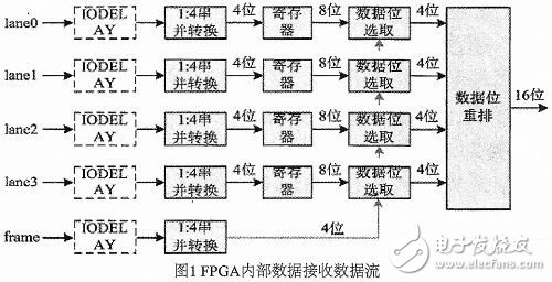
3 Data decoding After ensuring the integrity of the signal transmission and obtaining the correct serial data, serial-to-parallel conversion and data recombination are required to obtain the final sampled data. This process is implemented in the FPGA. ADS4 2LB69 supports 4-wire serial transmission. Each lane transmits 4bit data. The program structure of receiving ADC data in FPGA is shown in Figure 1. Serial data lane and frame clock (frame), first 1:4 serial and parallel conversion, data lane corresponds to 4bit data registration level and then output 8bit data (where the lower 4bit is the data D0 of one moment, the high 4bit is the latter The data D1) is latched at the moment, and the correct 4-bit data is obtained from the 8-bit registered data according to the 4-bit frame data. Finally, the four sets of 4-bit data are rearranged in the order of the ADC manual to obtain 16-bit sampled data.

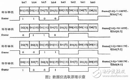
The 1:4 serial-to-parallel conversion is done using the FPGA internal ISERDES core. Since the time when the ISERDES core starts the serial-to-parallel conversion is uncertain, the converted 4-bit parallel frame data has four values, which respectively correspond to different data bit acquisition situations, as shown in FIG. 2 .

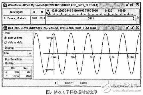
4 Experimental Verification In order to verify the correctness of the multi-bit LVDS data reception design, the data acquisition board was tested in the laboratory. The signal source is used to simulate the input signal and the sampling clock, and the sampled data after the internal rearrangement of the FPGA is uploaded to the PC through the JTAG test interface and displayed in the chipscope software. Figure 3 shows the test results when the sampling clock is 180MHz and the input signal frequency is 10MHz. Frame_ilatst is the frame clock data used to acquire the data bits, and data is the sampling data timing waveform. As the figure shows, the waveform is a single-frequency sine wave. Prove the correctness of the design.

5 Conclusion The correct reception of LVDS data from the overspeed ADC is critical to digital receivers. From the theoretical analysis and design implementation, this paper details how to achieve the correct reception of multi-bit high-speed LVDS data. The data acquisition board is designed by Xilinx FPGA and ADS42LB69, and the data receiving program is implemented in the FPGA. The experimental test shows that the hardware and program design can complete the correct reception of the sampled data. The method in this paper has certain guiding significance for similar ADC data receiving design.
Electrical Products,Upvc Pipe Fitting,Pvc Pipe Fittings,Pipe Fitting Flange,Pipe Clamp Fitting
FOSHAN SHUNDE LANGLI HARDWARE ELECTRICAL CO.LTD , https://www.langliplastic.com