The three magic weapons of the model electric engineer, have you learned these?
Differential signal 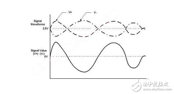
Differential transmission is a signal transmission technology. Different from the traditional one signal line and one ground line, differential transmission transmits signals on these two lines. The two signals have the same amplitude and opposite phase. The signals transmitted on these two lines are differential signals. The differential signal, also known as the differential mode signal, is relative to the common mode signal.
We use a method to compare differential signals. The differential signal is like two people on the seesaw. When one person is picked up, the other person is smashed down - but their average position is constant. To continue the analogy of the seesaw, a positive value can indicate that the person on the left is higher than the person on the right, while a negative value indicates that the person on the right is higher than the person on the left. 0 means that both people are at the same level. Applied to the electrical, the two jaws are represented by a pair of wires identified as V+ and V-.
CharacteristicsStrictly speaking, all voltage signals are differential because one voltage can only be relative to the other. In some systems, "system ground" is used as a voltage reference point. When 'ground' is used as a voltage measurement reference, this signal planning is called single-ended. We use this term because the signal is represented by the voltage on a single conductor. On the other hand, a differential signal acts on the two conductors. The signal value is the voltage difference between the two conductors. Although not necessary, the average of these two voltages will always be consistent.
It is conceivable that an equal voltage applied to the two conductors at the same time, the so-called common mode signal, has no effect on a differential amplification system, that is, although the input effective signal amplitude of a differential amplifier is only It takes a few millivolts, but it can be indifferent to a common-mode signal up to a few volts. This indicator is called the common-mode rejection ratio (CMRR) of the differential amplifier. The general op amp can reach more than 90db, and the high-precision op amp even reaches 120db. Since the interfering signal is generally in the form of a common mode signal, the application of the differential signal greatly increases the signal to noise ratio of the amplifier system.
advantage1. Strong anti-interference ability. Interference noise is generally equivalent and simultaneously loaded onto two signal lines with a difference of zero, ie, noise has no effect on the logical meaning of the signal.
2, can effectively suppress electromagnetic interference (EMI). Since the two wires are close together and the signal amplitudes are equal, the amplitudes of the coupled electromagnetic fields between the two wires and the ground wire are also equal, and their signals are opposite in polarity, and their electromagnetic fields cancel each other out. Therefore, the electromagnetic interference to the outside world is also small.
3. The timing is accurate. The receiving end of the differential signal is the point at which the difference between the amplitudes of the signals on the two lines is positive or negative, as the point at which the logic 0/1 jumps. The ordinary single-ended signal uses the threshold voltage as the trip point of the signal logic 0/1, which is greatly affected by the ratio of the threshold voltage to the signal amplitude voltage, and is not suitable for the low amplitude signal.
DisadvantageIf the area of ​​the board is very tight, the single-ended signal can have only one signal line, the ground line goes to the ground plane, and the differential signal must go two lines of equal length, equal width, close proximity, and at the same level. This often happens when the chip's pin spacing is so small that it can only pass through one trace.
Clock data recovery (CDR: clock data recovery)As a core function that high-speed serial communication must have, clock recovery is becoming more and more widely used. There are clock recovery modules in Ethernet, PCI-Express, and Aurora. In contrast, the traditional parallel transmission mode of clock and data cannot reach the bandwidth of 1 Gb/s or more.
Simply put, the so-called clock recovery is: according to the reference clock, the clock signal is extracted from the data signal. Correspondingly, only serial data is transmitted on the channel, and there is no clock signal on the channel. The data receiving end receives the serial data and performs clock recovery.
The basis of clock data recovery in SERDES
The CDR protocol typically runs at higher data rates and longer transmission distances, thus posing significant design challenges.
In the SERDES (Serializer-Deserializer) application, as the name implies, the CDR receiver must recover the embedded clock from the data. More precisely, the clock is obtained from the exchange of data signals.
The CDR Transmitter first transmits the data serially and then converts the data into an 8b/10b encoding scheme. The encoding process obtains 8-bit data and converts it into a 10-bit symbol. The 8b/10b encoding method can transmit an equal number of 0s and 1s on the data line, thereby reducing intersymbol interference and providing enough data edges for the receiver to lock the phase on the received data stream. The transmitter multiplies the system clock to the transmit bit rate and transmits 8b/10b data on the TX differential pair at that rate.
The task of the CDR receiver is first to lock the phase on the RX differential bit stream, then the receiver aligns the data bits according to the recovered clock and then uses the receiver's reference clock for word alignment. Finally, the data is decoded 8b/10b for use by the system.
In CDR systems, the transmit and receive systems typically have completely separate system clocks. These two clocks are critical in a particular range of variation, which is approximately hundreds of PPMs.
CDR circuit and jitter
The main design challenge of the CDR interface is jitter, the offset of the actual data transfer location relative to the desired location. Total jitter (TJ) consists of deterministic jitter and random jitter. Most jitter is deterministic, and its components include intersymbol interference, crosstalk, duty cycle, and period jitter (eg, interference from switching power supplies). Usually random jitter is a by-product of semiconductor heating problems and is difficult to predict.
The transmit reference clock, transmit PLL, serializer, and high-speed output buffer all affect the transmit jitter. For a given bit period or data eye, the transmission jitter is usually illustrated as a percentage of the unit interval or UI (unit interval). For example, the transmission jitter of the .2 UI indicates that the jitter consists of 20% of the bit period. For transfer jitter, the lower the UI values, the better, because they represent less jitter.
Likewise, the CDR receiver will specify the maximum amount of jitter that can be tolerated at a given bit rate. A typical bit error rate (BET) standard is 1e-12. Receive jitter is still specified by the UI. A larger UI indicates that the receiver can tolerate more jitter. A typical receiver specification is .8 UI, which means that 80% of the bit period can be noisy, and the receiver will still be able to receive data reliably. Jitter is usually quantified by a statistical bell-shaped distribution that has an ideal edge position at its fixed point.
Channel equalizationChannel equalization refers to an anti-fading measure taken to improve the transmission performance of a communication system in a fading channel. It is mainly to eliminate or reduce the inter-code crosstalk (ISI) problem caused by multipath delay in broadband communication.
The mechanism is to compensate for the characteristics of the channel or the entire transmission system. For the channel constant parameter or variable parameter characteristics, the data rate is different in size, and the equalization has multiple structural modes. Generally divided into two categories: linear and nonlinear equilibrium. The main difference between a linear equalizer and a nonlinear equalizer is that the output of the adaptive equalizer is used for feedback control. It is difficult to balance the channel with the communication channel. Generally, the baseband is equalized after demodulation at the receiving end, so the baseband equalization technique is widely used.In practice, an adaptive filter is generally added to achieve channel equalization. A filter is used to compensate for the distorted pulses, and the demodulated output samples obtained by the decider are samples that have been corrected by the equalizer or that have cleared the intersymbol interference. The adaptive equalizer continuously adjusts the gain from the actual digital signal transmitted according to an algorithm, and thus can adapt to the random variation of the channel, so that the equalizer always maintains an optimal state, thereby having better distortion compensation performance.
Portable Power Station also known as Portable Power Bank. Our product regulated DC Power, AC Pass-Through Charging, Wireless Fast Charger, Bluetooth Playback, Attentive Start, Car charger, Type-C ....... Large capacity meet the needs of all kinds of equipment.
Portable Power Station,Indoor Portable Power Station,Solar Portable Power Station,Portable Power Station With Bms
Jiangsu Zhitai New Energy Technology Co.,Ltd , https://www.zt-tek.com