Unknown RF test probe basics
Traditionally, RF probe contacts have been made with beryllium-copper (BeCu). Moreover, the earliest use of RF probe technology is very different from today's tools. After that, engineers made breakthroughs in probe technology to determine the basic requirements and working principles of RF probes.
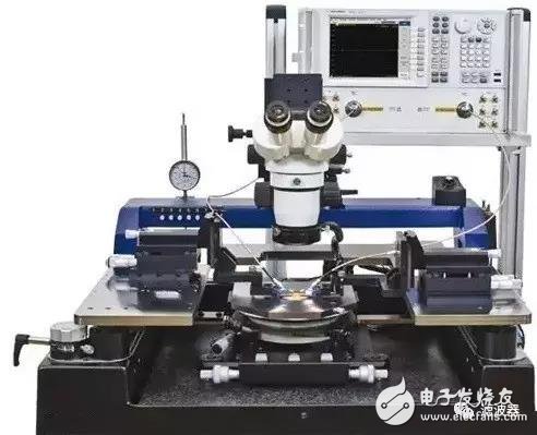
Radio frequency (RF) probes play an important role in almost every phase of the RF product life cycle: from technology development, model parameter extraction, design verification and commissioning to small-scale production testing and final production testing. By using RF probes, it is possible to measure the true characteristics of RF components at the wafer level. This can shorten research and development time and greatly reduce the cost of developing new products.
In just 30 years, RF probe technology has made amazing progress, from low frequency measurement to commercial solutions for a variety of applications: impedance matching in high frequency and high temperature environments at 110 GHz, multi-port, differential and Mixed-signal measurement devices, high-power measurements up to 60W in continuous wave mode, and terahertz applications up to 750GHz, can see RF probes.
The earliest use of RF probe technology is very different from today's tools. Early probes used a 50-Ω microstrip line that converges with a very short wire tip (wire TIp) through the probe substrate. A small hole is in contact with the pad of the device under test (DUT). At this time, the technical difficulty lies in how to achieve repeatable measurement when breaking through 4GHz. Although it is possible to eliminate the influence of a relatively large series inductance of a contact line tip by a calibration process, when the wafer holder is moved, the radiation resistance of the line tip may vary greatly. The pole tip design used for high frequency measurements is different from the pole tip for DC and low frequency measurements, and the 50-Ω environment must be as close as possible to the DUT pressure point.
The engineer then made a breakthrough in probe technology. The basic requirements and working principle of the RF probe are determined:
1) The 50-Ω planar transmission line of the probe should be in direct contact with the DUT pressure point without touching the conductor. For microstrip lines and subsequent coplanar probe designs, the probe contact is achieved with a small metal ball that is large enough to ensure reliable and repeatable contact.
2) In order to be able to simultaneously touch the signal pressure point and ground pressure point of the DUT, the probe needs to be tilted. This process is called "planarization of the probe."
3) The contact repeatability of the probe is much better than the repeatability of the coaxial connector. Facilitate the development of probe tip and on-chip standard and dedicated calibration methods.
4) A highly reproducible contact allows accurate calibration of the probe and moves the measurement reference plane towards its pole tip. The loss and reflection of the probe from the probe wire and the transition to the coaxial connector is offset by a similar error in the RF cable and connector.
5) Due to its small geometry, one can assume that the equivalent model of a planar standard is purely lumped. In addition, one can easily predict model parameters from the geometry of the standard part.
As the probe design changes from microstrip lines to coplanar waveguides (CPW), probe fabrication becomes easier (Figure 1). Tektronix eventually converted the probe from a “do-it-yourself†tool to a true product in the emerging RF semiconductor industry (Figure 2). This heralds the beginning of the era of wafer-level RF measurement.
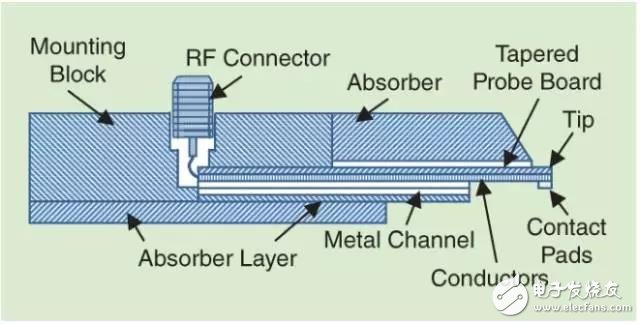
Figure 1 Wafer probe design based on ceramic coplanar line
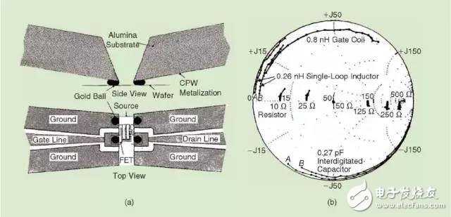
Figure 2 (a) Top view and side view of the coplanar probe
(b) One-port measurement of various on-chip impedance standard parts that have been modified
In the early 1980s, Tektronix introduced the first RF wafer probe model TMP9600 and the sapphire calibration substrate CAL96 (Figure 3). The main developers of the probes, Eric Strid and Reed Gleason, founded Cascade Microtech in 1983 and introduced the WPH probe. The two companies have provided very similar RF probes for several years, until Tektronix finally withdrew from the wafer probe business in the early 1990s. Under such an opportunity, CascadeMicrotech became the leading supplier of RF probes in the industry with its good relationship with Hewlett Packard.
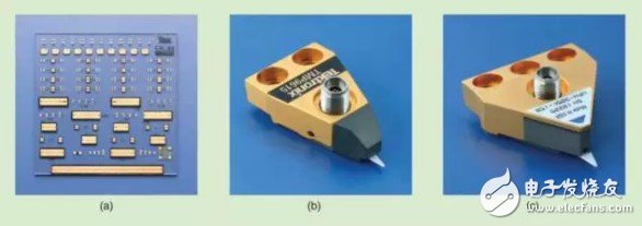
Figure 3 (a) The first commercial sapphire calibration substrate CAL96;
(b) RF round crystal probe TMP9600 from Tektronix;
(c) WPH probe from Cascade Microtech.
The frequency of the WPH probe was expanded to 26 GHz in a short period of time and reached 50 GHz in 1987 to meet the needs of rapidly developing monolithic microwave integrated circuits (MMICs). V-band and W-band probes appeared in 1991 and 1993, respectively. In 1988, Cascade introduced the 26.5GHz Series of Tip-Replaceable Probes (RTPs) for large-scale production applications. Now, people can quickly change the ceramic tip without moving the probe body from the test bench. The WPH probe contributed to the development of microwave technology in the 1980s and 1990s, but there are several technical limitations. The most critical limitation is the fragile ceramic CPW line. Even applying a minimum force above the recommended value (for example, to achieve better contact) can damage the probe. Many engineers call this moment "the voice of death." The sound of ceramic probe cracking often pushes the entire project to a dead end because probes are very expensive for universities and small laboratories. Although the RTP series was introduced, ceramic probes were squeezed out of the market by other technologies.
When GGB Industries patented a micro-coaxial cable-based RF probe, 1988 became another milestone. The use of micro-coaxial cables as intermediate transition media has the following benefits:
1) Significant mechanical improvements extend the life of the probe.
2) The damaged probe can be re-tapped in a relatively easy and inexpensive way.
3) Electrical characteristics have been improved.
4) Simplify the manufacturing process.
5) Reduce costs.
In 1993, GGB introduced W-band probes at the International Microwave Annual Conference (IMS) of the IEEE Theory and Technology Association. In 1999, their probes reached 220 GHz, and in 2006 they expanded further to 325 GHz and in 2012 reached 500 GHz. Together with close cooperation with suppliers such as Karl Suss (later SUSS MicroTech), GGB Industries has become one of the most influential companies in the global RF market.
At the same time, Cascade demonstrated the new 40-GHz air-coplanar probe (ACP) at the 43rd Spring ARFTG conference in 1994 (Figure 5). Within a few years, the ACP probe quickly reached 110 GHz (1-mm connector model) and 140 GHz (based on waveguide model), replacing the WPH line. So far, many engineers like to use ACP to detect gold pressure points due to the soft and non-destructive contact of ACP.
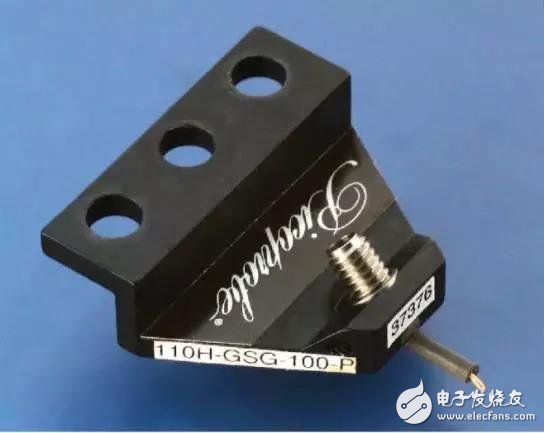
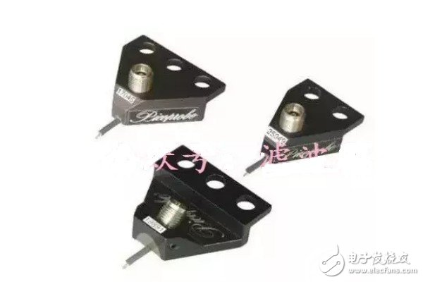
Figure 4 Picoprobe probe from GGB Industries
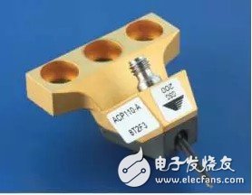
Figure 5 Cascade Microtech ACP Probe
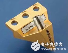
Figure 6 ∣Z∣-probe model.
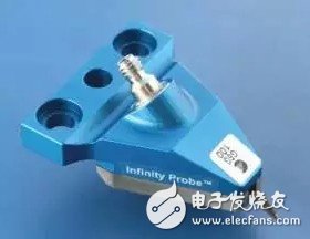
Figure 7 Cascade Microtech Infinity Probe
In 2000, Rosenberger launched a new concept for PCB applications with RF probes that significantly exceeded traditional technology, reducing the geometry of the probe to the level required by the wafer level and was introduced in 2001. New RF wafer probe ∣Z∣-probe. The ∣Z∣-probe can cover the 40 GHz range and implement several innovative ideas.
1) This probe does not use a micro coaxial cable. A direct transition from coaxial connection to air-insulated coplanar contact lines is achieved.
2) This transition is made in the probe body, which allows an accurate optimization of the transition point to minimize possible discontinuities.
3) Coplanar contact is fabricated using an ultraviolet lithography and electroplating process (UV-LIGA), which is similar to the process used to fabricate MEMS products. Its extremely high precision and repeatability form a very accurate shape of the CPW line and a constant air gap.
In the mid-1990s, silicon was heavily used in the RF field. This poses some challenges for the production of RF probes. Traditionally, RF probe contacts have been made with beryllium-copper (BeCu). This material becomes cumbersome when detecting the aluminum contact pressure points of silicon devices and circuits. The rapid oxidation of the BeCu tip and the accumulation of dirt can result in a significant reduction in contact repeatability at the aluminum contact pressure point. To solve this problem, the supplier provides an RF probe with a tungsten (W) pole tip. Test engineers operating multi-purpose measuring devices are forced to change probes each time they change the DUT type (silicon or III-V compound semiconductor), even if the frequency range of the test remains the same. The ∣Z∣-probe is also dedicated to solving this inconvenience. Coplanar contact is made of nickel (Ni) and exhibits optimum contact properties at contact pressures with aluminum and gold. Subsequently, suppliers of other RF probes have also begun to offer multi-purpose probes that use Ni or Ni alloys to make pole tips.
With the increasing RF requirements for MOS and BICMOS devices and the shrinking DUT contact point size, CascadeMicrotech introduced the basis for the AutomaTIc RF Techniques Group-ARFTG Microwave Measurement Conference in 2002. A new round crystal probe for thin film technology. This method is based on Cascade's Pyramid Probe Card technology. A microstrip line on a soft polyimide film substrate transmits signals from the coaxial line through the non-oxidized rare metal probe tip to the DUT. The contact area of ​​the Ni probe tip is approximately 12 μm x 12 μm, allowing for the detection of very small contact pressure points. This new Infinity probe demonstrates excellent contact consistency and probe-to-probe low crosstalk.
Cascade offers Infinity probes for different sizes at 110 GHz. Waveguide-based probes for 220 and 325 GHz measurements were introduced in 2005 and 2007, respectively. Cascade began offering Infinity probes for the 500 GHz-band in late 2009.
In 2009-2011, two new members entered the mature probe market: the DMPI with micromachined probes is aimed at the emerging sub-THz market. Allstron from Taiwan offers inexpensive probes for applications below 110 GHz, where lower test costs are the primary requirement. The probe from Allstron is a traditional design based on micro-coaxial cable. The contact structure is an air insulated CPW line. It is similar to ACP, but the pole tip is shaped to detect aluminum pressure points with a small passivation window (passivaTIon windows).
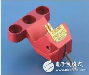
Figure 8 Allstron RF Probe
Modern designs for RF wafer probes convert test signals from a three-dimensional medium (coaxial cable or rectangular waveguide) to a two-dimensional (coplanar) probe contact. This operation requires careful handling of the characteristic impedance Z0 of the transmission medium and the correct conversion of electromagnetic energy between different propagation modes. Although the input to the wafer probe is a standardized coaxial or waveguide interface, its output (probe tip) allows for different design concepts. These interfaces, especially the tip of the probe, bring discontinuities into the measurement signal path. This discontinuity itself produces high-order propagation modes. Therefore, the round crystal probe and DUT excitation must support only a single quasi-TEM propagation mode and exclude higher order modes or exhibit higher impedance to higher order modes.
The conversion of the EM field profile is maintained by several RF transitions within a single probe assembly. A traditional RF probe consists of the following components:
1) Tester interface (coaxial or waveguide)
2) Transition from test interface to micro-coaxial cable
3) Transition from micro-coaxial cable to a planar waveguide, such as CPW or microstrip line
4) Coplanar interface (or pole tip) for the DUT on the wafer
Several probes either combine 3) and 4) or do not use a micro-coaxial cable (Figure 9). A coaxial connector is a commonly used test system interface for RF probes below 65 GHz. Both the coaxial and waveguide connections are possible interfaces in the 50 to 110 GHz frequency range. In a single scan, a broadband test system covering from DC to 110 GHz utilizes a minimum size (1 mm) coaxial connector. Different sizes of rectangular waveguides interface with measurement systems above 110 GHz.
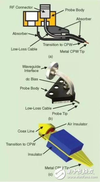
Figure 9 (a) RF probe based on a micro-coaxial cable
(b) Waveguide interface
(c) Direct transition from coaxial to coplanar
The natural life of a probe technology is about 12 years. There are two main factors driving the development of probe technology:
1) Improve measurement accuracy in high-end applications
2) Reduce the cost of testing for mainstream applications.
In addition to new probe suppliers for mainstream (Allstron) and high-end applications (DMPI), some small and medium-sized service providers in the RF microwave industry are also offering products for the low frequency and broadband sectors.
The MP series coaxial probes are provided to meet the measurement requirements of DC-20GHz. The characteristics are as follows:
1.DC-20GHz bandwidth
2. Ultra low insertion and return loss
3.GSG, GS configuration (0.8/1.5/2.5mm pitch range)
Advantage:
1. Easy to detect and test without any soldered board signal
2. Compatible pogo pin allows to explore non-planar structures
3. The life of the probe is longer
4. Less test time
Applied to:
1) RF and microwave module signal insertion, detection and measurement output;
2) Analysis of electrical performance of high frequency circuit boards;
3) Analysis of high speed digital circuits
5V power supply, it has multi plug were suitable for many countries. We can meet your specific requirement of the products, like label design. The plug type is US/UK/AU/EU. The material of this product is PC+ABS. All condition of our product is 100% brand new.
Our products built with input/output overvoltage protection, input/output overcurrent protection, over temperature protection, over power protection and short circuit protection. You can send more details of this product, so that we can offer best service to you!
5V Power Supply,5V Pc Power Supply,5V Dc Power Supply ,5V Power Supply For Computer
Shenzhen Waweis Technology Co., Ltd. , https://www.huaweishiadapter.com