A narrow pulse small signal operation amplifying circuit which is formed by cascading three chips
Abstract : A narrow pulse small-signal op amp circuit is designed and implemented in the paper. At the beginning of the article, we first introduced the background of the op amp and the purpose of the design, then introduced the design ideas and specific circuit implementation, and finally tested the op amp. Tests have shown that the op amp can amplify a narrow pulse small signal with a rising edge of 50 ns.
An operational amplifier is a circuit unit with a very high amplification factor. In an actual circuit, a feedback function is usually combined with a feedback network to form a certain functional module. Since it was first used in analog computers to implement mathematical operations, it was named "Operational Amplifier". The op amp is a circuit unit named from a functional point of view, which can be implemented by discrete devices or in semiconductor chips. With the development of semiconductor technology, most of the op amps exist in the form of a single chip. There are many types of op amps, which are widely used in the electronics industry.
The paper introduces a differential operational amplifier with three chips cascaded. The op amp can achieve narrow pulse small signal amplification, and the rising edge of the pulse can reach 50 ns.
1 Design purposeAccording to the needs of the project, the differential op amp designed this time is used to amplify the signal output from the detector. Since the signal received by the receiver is small signal pulse modulation, the designed op amp must be able to amplify the small signal narrow pulse. Because in the case of small signals, the detector output is in the millivolt level, and the index requires the output to be between -2 and +2V, the differential amplifier circuit is designed to be approximately 100 times larger.
2 Design ideasSince the op amp is designed to amplify the pulse signal, the rising edge of the pulse signal must be considered. If the rising edge time is too large, the pulse signal will be distorted. Therefore, the design is initially limited to the pulse signal rising edge time T. <50 ns. Since the bandwidth and rising edge of the pulse signal have the following relationship: F ​​& TImes; T = 3.5 (F represents the bandwidth), it can be seen that the smaller the rising edge time, the larger the bandwidth, when the rising edge time T = 50 ns. The bandwidth is up to 70MHz. Because the bandwidth and gain of the op amp are inversely proportional, if only the first-level op amp is used, the gain will not reach the required 100 while achieving the required bandwidth. Therefore, the op amp of this design uses two-stage amplification. Structure, 10 times magnification per stage.
3 related circuitsFrom the above analysis, it can be known that the operational amplifier circuit adopts a two-stage structure. The first stage first differentially amplifies the baseband signal. The chip selects the ADA4817-1 and ADA4817-2 of AD Company. The first stage amplification circuit is shown in Figure 1.
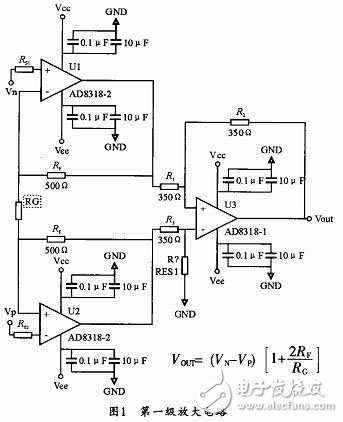
The ADA4817-1 (single-channel) and ADA4817-2 (dual-channel) FastFET amplifiers used in the first stage of amplification are unity-gain stable, ultra-high-speed voltage feedback amplifiers with FET inputs. These amplifiers use ADI's proprietary Ultra High Speed ​​Complementary Bipolar (XFCB) process, which enables high speed and ultra low noise (4nV/√Hz; 2.5 fA/√Hz) and extremely high input impedance. .
The signal outputted by the first stage is secondarily amplified, and the second stage is amplified by the AD8009 chip of AD company. Figure 2 shows the second stage amplifying circuit.
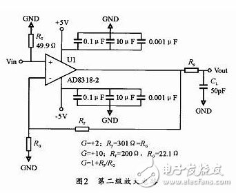
The AD8009 chip for second-stage amplification is an ultra-high-speed current-feedback amplifier with an impressive slew rate of 5 500 V/μs and a rise time of only 545 ps, making it ideal for use as a pulse amplifier.
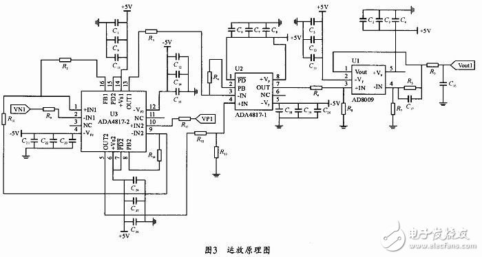
In addition, in order to prevent self-excitation, a 10Ω resistor is connected in the middle of the two-stage amplification. Figure 3 is an overall schematic diagram of a differential op amp.
In summary, it is shown that the op amp has almost no distortion, and the millivolt-level narrow pulse small signal output by the detector is amplified by nearly 100 times. This proves that the differential op amp of this design is able to meet the requirements and has good performance.
300-500 Kw Marine Diesel Engine
300-500 Kw Marine Diesel Engine,Marine Engine,6190 Diesel Engine,300Kw Marine Diesel Engine
Jinan Guohua Green Power Equipment Co.,Ltd. , https://www.guohuagenerator.com