A text teaches you to quickly master the AT89C51 microcontroller (including actual development case)
AT89C51 is a low voltage, high performance CMOS 8-bit microprocessor with 4K bytes of FLASH memory (FPEROM - Flash Programmable and Erasable Read Only Memory), commonly known as microcontroller. The AT89C2051 is a microcontroller with 2K bytes of Flash programmable erasable read-only memory. The erasable read-only memory of the microcontroller can be erased 1000 times repeatedly. The device is fabricated using ATMEL high-density non-volatile memory fabrication technology and is compatible with the industry-standard MCS-51 instruction set and output pins. With the combination of a versatile 8-bit CPU and flash memory in a single chip, ATMEL's AT89C51 is a highly efficient microcontroller, and the AT89C2051 is a streamlined version. The AT89C51 microcontroller provides a flexible and inexpensive solution for many embedded control systems. The shape and pinout are as shown.
2. The main features of AT89C51
· Compatible with MCS-51 · 4K byte programmable flash memory life: 1000 write / wipe cycle data retention time: 10 years · full static operation: 0Hz-24Hz
· Three-level program memory lock · 128*8-bit internal RAM
32 programmable I/O lines · two 16-bit timer/counters · 5 interrupt sources · programmable serial channels · low power idle and power-down modes · on-chip oscillator and clock circuit
3.AT89C51, AT89C52 and AT89S51 three kinds of single chip shape
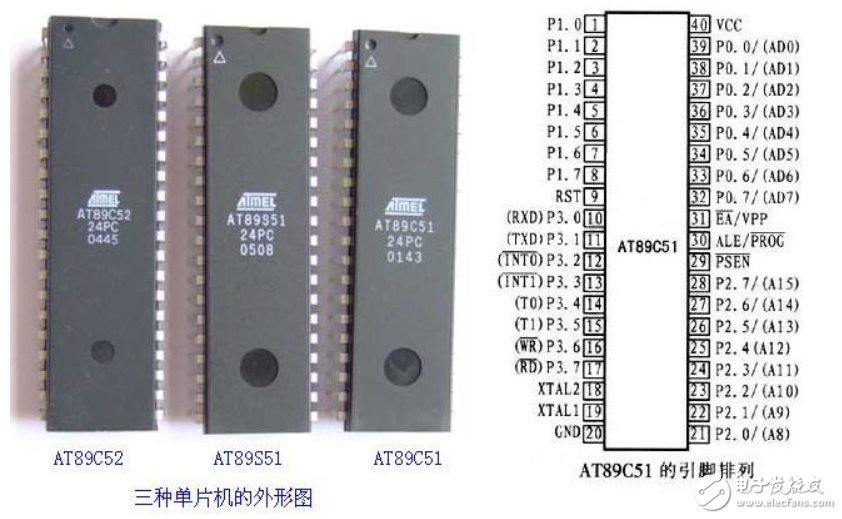
4. AT89C51 pin description:
VCC: Supply voltage.
GND: Ground.
P0 port: P0 port is an 8-bit drain open bidirectional I/O port, which can absorb 8TTL gate current per pin. When the pin of the P1 port writes 1 for the first time, it is defined as a high-impedance input. P0 can be used for external program data memory, which can be defined as the eighth bit of data/address. In FIASH programming, P0 port is used as the original code input port. When FIASH performs verification, P0 outputs the original code. At this time, P0 must be pulled high.
P1 port: P1 port is an 8-bit bidirectional I/O port with pull-up resistor inside. P1 port buffer can receive 4TTL gate current. After the P1 port pin is written to 1, it is internally pulled up high and can be used as an input. When the P1 port is pulled low externally, it will output current, which is due to internal pull-up. In FLASH programming and verification, the P1 port is received as the eighth bit address.
P2 port: P2 port is an 8-bit bidirectional I/O port with internal pull-up resistor. P2 port buffer can receive and output 4 TTL gate currents. When P2 port is written “1â€, its pin is internally The pull resistor is pulled high and is used as an input. Therefore, when the input is made, the pin of the P2 port is pulled low externally, and the current will be output. This is due to internal pull-ups. When the P2 port is used for external program memory or 16-bit address external data memory for access, the P2 port outputs the upper eight bits of the address. When the address "1" is given, it takes advantage of the internal pull-up. When reading and writing to the external eight-bit address data memory, the P2 port outputs the contents of its special function register. The P2 port receives the upper eight address signals and control signals during FLASH programming and verification.
P3 port: P3 port pin is 8 bidirectional I/O ports with internal pull-up resistors, which can receive and output 4 TTL gate currents. When the P3 port is written to "1", they are internally pulled up high and used as inputs. As an input, since the external pull-down is low, the P3 port will output current (ILL) due to the pull-up. P3 port can also be used as some special function ports of AT89C51, as shown in the following table:
Port pin optional function
P3.0 RXD (serial input port)
P3.1 TXD (serial output port)
P3.2 /INT0 (external interrupt 0)
P3.3 /INT1 (external interrupt 1)
P3.4 T0 (timer 0 external input)
P3.5 T1 (Timer 1 external input)
P3.6 /WR (external data memory write strobe)
P3.7 / RD (external data memory read strobe)
The P3 port receives some control signals for both flash programming and program verification. RST: Reset input. When the oscillator resets the device, keep the RST pin high for two machine cycles.
ALE/PROG: When accessing external memory, the output level allowed by the address latch is used to latch the status byte of the address. This pin is used to input the programming pulse during FLASH programming. In normal times, the ALE terminal outputs a positive pulse signal at a constant frequency cycle, which is 1/6 of the oscillator frequency. It can therefore be used as a pulse for external output or for timing purposes. However, it should be noted that an ALE pulse will be skipped whenever used as an external data memory. If you want to disable the output of ALE, you can set it to 0 on the SFR8EH address. At this time, ALE only works when MOVX is executed, and MOVC instruction is ALE. In addition, this pin is pulled slightly higher. If the microprocessor is in the external execution state ALE inhibit, the set is invalid. /PSEN: Strobe signal for external program memory. During the fetch by the external program memory, each machine cycle is active twice / PSEN. However, when accessing the external data memory, these two valid /PSEN signals will not appear.
/EA/VPP: When /EA is held low, then the external program memory (0000H-FFFFH) during this period, regardless of whether there is internal program memory. Note that when Encryption Mode 1 is selected, /EA will be internally locked to RESET; when /EA is held high, this is the internal program memory. This pin is also used to apply 12V programming power (VPP) during FLASH programming.
XTAL1: Input to the inverting oscillator amplifier and input to the internal clock operating circuit.
XTAL2: Output from the inverting oscillator.
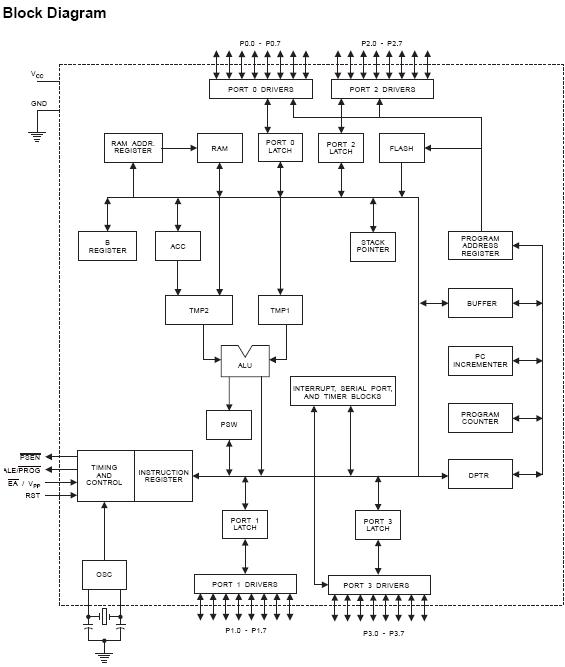
AT89C51 internal function diagram:
3. Oscillator Characteristics: XTAL1 and XTAL2 are the input and output of the inverting amplifier, respectively. The inverting amplifier can be configured as an on-chip oscillator. Both rock crystal oscillation and ceramic oscillation can be used. If an external clock source is used to drive the device, XTAL2 should not be connected. The input to the internal clock signal is passed through a two-way flip-flop, so there is no requirement for the pulse width of the external clock signal, but the width required for the high and low levels of the pulse must be guaranteed.
4. Chip Erase: The electrical erase of the entire PEROM array and the three lock bits can be accomplished by combining the correct control signals and keeping the ALE pin low for 10ms. In a chip erase operation, the code array is all written "1" and the operation must be performed before any non-empty memory bytes are repeatedly programmed.
In addition, the AT89C51 features steady-state logic that can be used for static logic at low to zero frequencies, supporting two software-selectable power-down modes. In idle mode, the CPU stops working. But RAM, timers, counters, serial ports and interrupt systems are still working. In power-down mode, the contents of the RAM are saved and the oscillator is frozen, disabling other chip functions used until the next hardware reset.
89s51 is an upgraded version of 89c51, 89SXX can be backward compatible with 51 series chips such as 89CXX. The differences are as follows:
1, 89S51 has been improved in the process, 89S51 uses 0.35 new technology, the cost is reduced, and the function is improved, increasing the competitiveness.
2, a lot of new features, performance has been greatly improved.
3, 89s51 has ISP online programming function, the advantage of this function is that rewriting the program in the MCU memory does not need to strip the chip from the working environment. The speed is faster, the stability is better, and the programming voltage only needs 4~5V.
4. The highest working frequency is 33MHz, and the limit working frequency of 89C51 is 24M.
5, 89s51 has a duplex UART serial channel.
6, 89s51 internal integrated watchdog timer, no need to external watchdog timer unit circuit like 89C51.
7, 89s51 with a double data indicator.
8, 89s51 with power off indicator.
9, 89s51 with a new encryption algorithm, which makes the crack of the 89S51 impossible, the confidentiality of the program is greatly enhanced, so that the protection of intellectual property rights can not be effectively violated.
10, power range: 89S5 * power range is as wide as 4 ~ 5.5V, and 89C5 * series can not work properly below 4.8V and above 5.3V.
11. Longer programming life: 89S5* nominal 1000 times, the actual minimum is 1000 times to 10000 times, which is more favorable for beginners to repeatedly write and reduce learning costs.
The most popular related development case of AT89C51 microcontroller
1. Intelligent pedometer design based on AT89C51 single chip microcomputer
The pedometer consists of an oscillating circuit, a reset circuit, a display circuit, and a button circuit, and is powered by a battery. The system structure diagram is shown in Figure 1.
Figure 1 system structure diagram
For details, please refer to the design of intelligent pedometer based on AT89C51 single chip microcomputer.
2. Using AT89C51 single-chip microcomputer to control the assembly source of stepper motor
Source program
SPEED EQU 10H ; SPEED is the speed grade mark, a total of 7 levels, ie 1~7
FX EQU 11H ; FX for direction sign
COUNT EQU 12H ; COUNT Interrupts Sign
ORG 0000H
AJMP MAIN
ORG 0003H; external interrupt 0 entry address, acceleration subroutine
AJMP UP
ORG 0013H; external interrupt 1 entry address, deceleration subroutine
For details, please refer to: Using AT89C51 MCU to Control the Assembly Source of Stepper Motor
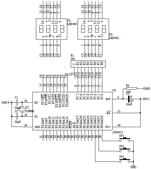
3.at89c51 electronic clock circuit diagram and program
At89c51 electronic clock circuit diagram:
1. Function:
1 When the power is turned on, the time from 12:00:00 is displayed;
2 P0.0/AD0 controls the adjustment of “secondsâ€, each press is added for 1 second;
3 P0.1/AD1 controls the adjustment of “minutesâ€, adding 1 point for each press;
4 P0.2/AD2 controls the “time†adjustment, each time you press 1 hour;
Source program:
3. Hardware connection on the system board (1) Connect the P1.0-P1.7 port in the "Microcontroller System" area to the A-H port in the "Dynamic Digital Display" area with an 8-pin cable;(2) Connect the P3.0-P3.7 port in the SCM system: the 8-pin cable to the S1-S8 port in the “Dynamic Digital Display†area;
(3) Connect the P0.0/AD0, P0.1/AD1, P0.2/AD2 ports in the “Single-Chip System†area to the SP3, SP2, and SP1 ports in the “stand-alone keyboard†area.
For details, please refer to: at89c51 electronic clock circuit diagram and program
4. Design of electric bicycle fast charger based on AT89C51
The pulse charging mode means that the pulse current intermittently charges the battery, the charging pulse makes the battery full of electricity, and the intermittent period causes the oxygen and hydrogen generated by the chemical reaction of the battery to be recombined and absorbed, and the polarization is eliminated to reduce the internal pressure of the battery. The constant current charging of the next pulse can be smoothly performed, so that the battery can absorb more power. The intermittent pulse makes the battery have a sufficient reaction time, reduces the gassing amount, and improves the charging current acceptance rate of the battery.
Third, the system consists of
The main circuit of the charger adopts a half-bridge conversion type high-frequency switching power supply, and the control circuit is realized by a single chip microcomputer. After removing the common mode signal through the EMI filter, the grid alternating current is bridge rectified, and then connected to the two switching tubes V1 and V2 through the two capacitors to convert the sinusoidal alternating voltage into a pulse voltage higher than the charging voltage. After a half bridge filter and LC filter circuit, the voltage reaches a relatively stable value. The control circuit is composed of single-chip AT89C51, and the power supply is provided by the grid AC through transformer transformer, full-bridge rectification, and voltage regulator. The MCU controls the output pulse in a software manner by detecting the voltage signal of the temperature sensor, thereby controlling the on and off of the switch tube. In addition, by detecting the charging voltage and current value, the output pulse width of the microcontroller is controlled to enter different charging stages.
5. Design of intelligent regulated power supply based on AT89C51 This paper introduces a design scheme of intelligent regulated power supply based on AT89C51. Its core technology is to control the output of the voltage regulator module after controlling digital-to-analog conversion by AT89C51. The system consists of a rectification and filtering preliminary voltage regulator circuit, an AT89C51 control part, a DAC and a display part. The regulated power supply can be continuously step-adjustable and can be displayed in real time to make up for the shortcomings of the traditional regulated power supply.
The DC stabilized power supply studied by this system is mainly in line with the characteristics of intelligence, digitization and modularization: intelligent means that the system has programmable modules to intelligently control the system; digitization means that the system output voltage is displayed through the 7-segment digital tube, and The output voltage is continuously stepped digitally adjusted by pressing the button; the modular finger system is composed of various related modules, which improves the reliability of the system.
AT89C51 intelligent regulated power supply design principle
1, design system block diagram
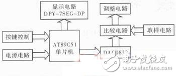
The system consists of modules, and the system block diagram of its modules is shown in Figure 1.
ShenZhen Antenk Electronics Co,Ltd , https://www.antenkcon.com