Teach you how to improve the luminous efficiency of LED
Principle of LED illumination The core of the LED is a PN junction, so it has the current-voltage characteristics of a general PN junction, ie, forward conduction, reverse cut-off or breakdown characteristics. In addition, it has luminescent properties under certain conditions. At the forward voltage, electrons are injected into the P region from the N region, and holes are injected into the N region from the P region. A part of the minority carriers (small children) entering the other area is combined with the majority carriers (multiple sub-groups) to emit light, as shown in Fig. 1. Since the recombination emits light in the minority carrier diffusion region, light is generated only within a few micrometers of the PN junction surface. There are several mechanisms that affect the forward voltage level, including contact resistance, transparent conductive layers, and carrier concentration and carrier mobility in P-type and N-type semiconductors.
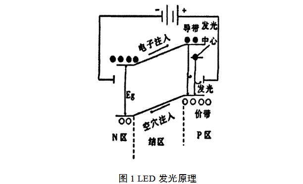
Assuming that luminescence occurs in the P region, the injected electrons directly composite with the valence band holes to emit light, or are first captured by the luminescent center and then condensed with the holes. Semiconductor materials with different chemical compositions, based on the different energy gap values ​​they have, can be combined to obtain light-emitting diodes of different emission wavelengths.
LED luminous efficiency description 1. Internal quantum efficiency electrons and holes recombine in the PN junction transition layer to generate photons. However, not every pair of electrons and holes will generate photons. Since the PN junction of the LED acts as an impurity semiconductor, there is a material. Quality, dislocation factors, and various defects in the process can cause problems such as ionization of ions, excitation scattering, and lattice scattering, which cause non-radiative transitions when electrons are exchanged from an excited state to a ground state and exchange energy with lattice atoms or ions. That is, no photons are generated. This part of energy is not converted into light energy and converted into thermal energy loss in the PN junction, so there is a composite carrier conversion efficiency. Of course, it is difficult to calculate the total number of composite carriers and the total number of photons produced. This efficiency is generally evaluated by measuring the optical power of the LED output. This efficiency is called internal quantum efficiency. Use symbols to teach you how to improve the luminous efficiency of LEDs:

2. The photons generated by the external quantum efficiency radiation composite can not all exit from the crystal, and the photons generated from the active region can be reabsorbed through the semiconductor; in addition, due to the high refractive index of the semiconductor, the photons are at the interface. It is easy to cause total reflection and return to the inside of the crystal. Even photons that are incident perpendicularly to the interface produce high reflectivity due to the high refractive index, and a considerable portion is returned to the inside of the crystal. Therefore, the external quantum efficiency can be expressed as:

Generally, LEDs are grown in a planar structure on a substrate having a light absorbing function, and are encapsulated in an epoxy dome shape. The light extraction efficiency of this structure is very low, only about 4%, so only a small portion of light is used. The main reasons for being released are: first, improper current distribution and absorption of light by the material itself; second, light is not easily transmitted from a high refractive index semiconductor to a low refractive index peripheral air (n = 1). Due to the high refractive index of the LED material, when the chip emits light at the interface between the crystal material and the air, total reflection occurs, and the crystal itself absorbs a considerable portion of the folded light, thus greatly reducing the external light extraction efficiency.
Five factors affecting LED luminous efficiency
Let us look at the reasons why temperature affects LED light efficiency, including the following:
(1) As the temperature rises, the concentration of electrons and holes increases, the band gap decreases, and the electron mobility decreases.
(2) When the temperature rises, the probability of recombination of electrons and holes in the potential well decreases, resulting in non-radiative recombination (heat generation), thereby reducing the internal quantum efficiency of the LED.
(3) The temperature rise causes the blue light peak of the chip to shift toward the long wave direction, so that the emission wavelength of the chip and the excitation wavelength of the phosphor do not match, which also causes the external light extraction efficiency of the white LED to decrease.
(4) As the temperature rises, the quantum efficiency of the phosphor decreases, the light emission decreases, and the external light extraction efficiency of the LED decreases.
(5) The performance of silica gel is greatly affected by the ambient temperature. As the temperature increases, the thermal stress inside the silica gel increases, causing the refractive index of the silica gel to decrease, thereby affecting the LED light effect.
In general, the effect of the decrease in luminous flux with increasing junction temperature is reversible. That is to say, when the temperature returns to the initial temperature, the light output flux will have a recovery growth. This is because some of the relevant parameters of the material will change with temperature, resulting in changes in the parameters of the LED device, affecting the light output of the LED. When the temperature returns to the initial state, the LED device parameters change and the LED light output returns to the initial state. In this regard, the luminous flux values ​​of the LEDs are divided into "cold lumens" and "heat lumens", respectively indicating the light output of the LEDs at room temperature and at a certain temperature.

How to improve the luminous efficiency of LEDs Early development of LED components focused on improving their internal quantum efficiency. The main method is to improve the quality of the chip and change the structure of the chip, so that the electrical energy is not easily converted into thermal energy, thereby indirectly improving the luminous efficiency of the LED. A theoretical internal quantum efficiency of about 70%. With the development of epitaxial growth technology and multi-quantum well structure, the internal quantum efficiency of ultra-high brightness LEDs has been greatly improved. For example, the internal quantum efficiency of wavelength 625 nm AlGalnP-based ultra-high brightness LEDs can reach 100%. Close to the limit.
The photoelectric conversion efficiency of the semiconductor material itself is far higher than other illuminating light sources, so now increasing the external quantum efficiency of the chip is the key to improving the luminous efficiency. The main technical approaches and developments adopted at home and abroad are as follows:
1. Technology for changing the shape of the chip Krarnnes et al. used a special tool to make the AlInGaP red LED tabletop into a flat-topped pyramid (TIP) chip, which was bonded to the transparent substrate to achieve an external quantum efficiency of more than 50%. The TIP structure reduces the transmission distance of light in the crystal, reduces the optical loss caused by internal reflection and absorption (active region absorption and free interceptor absorption, etc.), and greatly improves the chip characteristics, and the luminous efficiency reaches 100 lm/W (100 mA). , 610nm), the external quantum efficiency is up to 55% (650nm), while the face-down flip-chip structure makes the PN junction closer to the heat sink, improving the heat dissipation characteristics and improving the chip life. For conventional positive-load GaN-based LEDs, the chip can be etched 23 using wet etching. The sidewall tilt angle is used to increase the light extraction efficiency, and this method has now been mass-produced. The light emitted by the active layer of the LED is omnidirectional, and part of the light is emitted in the horizontal direction due to the relationship of refraction or reflection. This part of the light only increases the divergence of the light and the luminous efficiency of the element. Without much help, the light should be emitted more from the front. In GaN-based LEDs, according to Snell's law, how to improve the luminous efficiency of LEDs, that is, the critical angle of refraction is about 23 by the formula. Therefore, H3P04 and H2S04 mixed solution can be used and wet etching can be used to form a sidewall angle of about 23* with the vertical side at a certain temperature to change the light transmission direction and cause light to be emitted from the front side. The brightness is more concentrated and the brightness is improved. In this way, the total side reflection probability of the light can be increased, and the result is shown in FIG. This allows the brightness of the device to be more concentrated and the brightness to be improved.
Teach you how to improve the luminous efficiency of LEDs 2. Flip-chip technology GaN-based diode epitaxial wafers are generally grown on an insulating sapphire substrate. The ohmic contact P and N electrodes can only be fabricated on the same side of the epitaxial surface. The light portion will be blocked by the contact electrode and the bond wire. The main cause of light absorption is that the conductivity of the P-type GaN layer is low. To meet the requirements of current spreading, the thickness of the translucent Ni-Au ohmic contact layer covering most of the surface of the epitaxial layer should be greater than 5-10 nm, but To minimize light absorption, the thickness of the Ni-Au ohmic contact layer must be very thin, so that a proper compromise should be given between the transmittance and the extended resistivity. The result of the compromise design must increase the power conversion. Limited. In 2001, Lumileds reported the application of flip-chip bonding technology on high-power AlnGaN-based chips, which avoids the influence of electrode pads and leads on light extraction efficiency, improves current diffusivity and heat dissipation, and the preparation of back-reflective film will be transmitted. The light below reflects back to the sapphire side of the light, further improving the light efficiency, external quantum efficiency of 21%, power conversion efficiency of 20% (20mA, 435nm), maximum power up to 400mW (drive current 1A, 435nm, chip size lmm* Lmm), its overall luminous efficiency increased by 1.6 times than the formal wear.
3. Growth distribution Bragg reflection layer (DBR) structure The GaN-based chip with DBR layer is grown by epitaxial technique. DBR is a layered structure in which two kinds of materials with different refractive indices are alternately grown periodically, which is between the active layer and the substrate. The light that is incident on the substrate can be reflected back to the surface or the side surface, which can reduce the absorption of light by the substrate and improve the light extraction efficiency. However, since the DBR reflectivity decreases rapidly with the increase of the incident angle, the omnidirectional average still has a high optical loss, and the reflective film is not efficient.
4. Surface roughening technology Surface roughening mainly changes the direction of light that satisfies the law of total reflection, and then passes through the interface without being totally reflected on the other surface or reflected back to the original surface, and can function as anti-reflection. Such a method was first proposed by Nichia Chemical Co., Ltd. The roughening method basically forms a regular concave-convex shape on the geometry of the component, and the structure of the regular distribution is divided into two forms according to the position. One is to provide a concave-convex shape in the assembly, and the other is to make a regular concave-convex shape above the assembly and a reflective layer on the back of the assembly. Since the uneven shape can be provided at the interface of the GaN-based compound semiconductor layer by using a conventional process, the above-described first mode has high practicability. At present, if an ultraviolet component with a wavelength of 405 nm is used, an external quantum efficiency of 43% can be obtained, and the extraction efficiency is 60%, which is the highest external quantum efficiency and extraction efficiency in the world. In 1999, Fuji reported that an AlInGaN-based chip was bonded to a silicon substrate, and the substrate was removed by laser lift-off. The surface of the n-type GaN was photoetched by photoelectrochemical etching to form an ordered tapered shape to increase the luminescence intensity by 2.3 times.
5, photonic crystal technology shallow two-dimensional surface grating photonic crystal can avoid damage to the active area and introduce too much surface damage in the photonic crystal preparation process, causing the decline of internal quantum efficiency, while at the same time can play the diffraction effect of photonic crystal, Changing the incident angle of light increases the light efficiency by 1.7 to 2.7 times. The fabrication process involves electron beam lithography or other etching processes.
Do you know which is the most competitive student laptop for elementary students or daily entertainment? It`s this 14.1 inch celeron n4020 64gb laptops on sale for students, since not only lightweight, but also entry celeron cpu, storage, longer lasting battery, etc. More than 80% clients choose this student chromebooks for students tender cause it`s of all features of laptop for online classes. Of course, this model is also suitable for operating student laptop deals.
As a professional oem&ODM manufacture, never let you down. No matter you look for 14inch 64gb student pc, 15.6 inch N5095 Teacher Laptop, 15.6 inch 10th or 11th University Laptop, 16.1 inch 4gb graphics recommended laptop for programming, Android Tablet, Mini PC or All In One PC , always have the right one here for you.
Therefore, just feel free to contact us and share your basic requirement, like size, cpu, ram, rm, quantity, special requirements, so that send back right details for you.
Student Laptop,Student Laptop Deals,Laptops On Sale For Students,Student Pc,Laptop For Online Classes
Henan Shuyi Electronics Co., Ltd. , https://www.shuyilaptop.com